Programmable Unijunction Transistor:
PUT Operation – The Programmable Unijunction Transistor (PUT) is actually an SCR-type device used to simulate a UJT. The interbase resistance (RBB) and the intrinsic standoff ratio (η) can be programmed to any desired values by selecting two resistors. This means that the device Ming voltage (the peak voltage VP) can also be programmed.
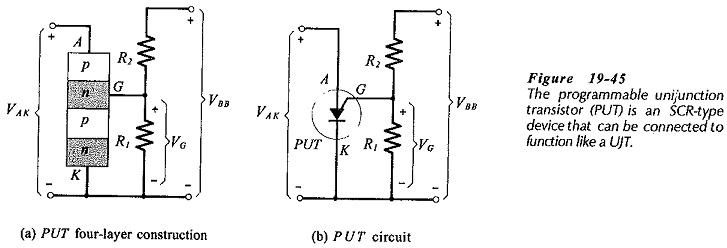
Consider Fig. 19-45(a) which shows a four-layer device with its gate connected to the junction of resistors R1 and R2. Note that the gate terminal is close to the anode of the device, instead of the cathode as for an SCR. The anode-gate junction becomes forward biased when the anode is positive with respect to the gate. When this occurs, the device is triggered on.
anode-to-cathode voltage then drops to a low level, and the PUT conducts heavily until the current becomes too low to sustain conduction. To simulate the UJT performance, the anode of the device acts as the UJT emitter, and R1 and R2 operate as rB1 and rB2, respectively. Parameters RBB, η, and VP are programmed by selection of R1 and R2. The four-layer block diagram is replaced with the PUT graphic symbol in Fig. 19-45(b). Note that this is the same as the SCR symbol except that the gate terminal is at the anode.
PUT Characteristics:
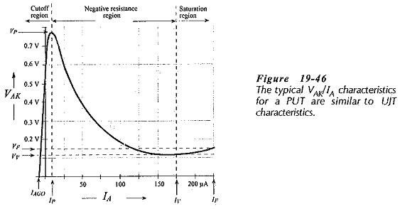
The typical PUT characteristic (VAK plotted versus IA) shown in Fig. 19-46 are seen to be very similar to UJT characteristics. A small gate reverse current (IAG0) flows while the anode-gate junction is reverse biased. At this point the PUT is in the cutoff region of the characteristics.
When the anode voltage is raised sufficiently above the gate voltage (VG in Fig. 19-45), the PUT is triggered into the negative resistance region of its characteristics, and the anode-cathode voltage falls rapidly to the valley voltage (VV). Further increase in IA causes the device to operate in its saturation region.
PUT Parameters:
The intrinsic standoff ratio for the PUT is,
![]()
The gate voltage is simply,
![]()
and the peak voltage is,
![]()
where VD is the anode-gate junction voltage, typically 0.7 V.
The gate source resistance (RG) is an important quantity because it affects the peak current and valley current for the PUT. RG is the resistance at the junction of voltage divider R1 and R2, (Fig. 19-45).