8253 Programmable Interval Timer:
8253 Programmable Interval Timer – In the process control system or automation industry, a number of operations are generally performed sequentially. Between two operations, a fixed time delay is specified. In a microprocessor-based system, time delay can be generated using software. Sequences of operations are also performed based on software. Therefore time delay, sequence and counting can be done under the control of a microprocessor. These most common problems can be solved using the 8253 in any microcomputer system.
The 8253 Programmable Interval Timer/counter specifically designed for use in real-time application for timing and counting function such as binary counting, generation of accurate time delay, generation of square wave, rate generation, hardware/software triggered strobe signal, one-shot signal of desired width, etc. The function of 8253 timer is that of a general purpose, multi-timing element which can be treated as an array of I/O ports in the system software.
The generation of accurate time delay using software control or writing instruction is possible. But instead of writing instructions for time delay loop, the 8253 timer may be used for this. The programmer configures the 8253 as per requirements. When the counters of the 8253 are initializing with the desired control word, the counter operates as per requirement. Then a command is given to the 8253 to count out the delay and interrupt the CPU. At the instant it has completed its tasks, the output will be obtained from the output terminal. Multiple delays can easily be implemented by assignment of priority levels in the microprocessor.
The counter/timer can also used for non-delay in nature such as Programmable Rate Generator, Event Counter, Binary Rate Multiplier, Real Time Clock, Digital One-Shot, and Complex Motor Controller. The 8253 operates in the frequency range of dc to 2.6 MHz while the 8253 use NMOS technology. The 8253 is compatible to the 8085 microprocessor. Generally, 8253 Programmable Interval Timer can be operating in the following modes.
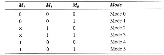
- Mode 0 Interrupt on terminal count
- Mode 1 Programmable one-shot
- Mode 2 Rate generator
- Mode 3 Square-wave generator
- Mode 4 Software triggered mode
- Mode 5 Hardware triggered mode
The pin diagram, block diagram of 8253, interfacing with 8085 microprocessor and operation of each mode have been explained in this section.
Pin Diagram of 8253
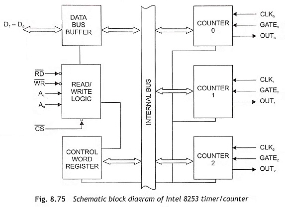
The 8253 timer is a 24-pin IC and operates at +5 V dc. It consists of three independent programmable 16-bit counters: Counter 0, Counter 1, and Counter 2. Each counter operates as a 16-bit down counter and each counter consists of clock input, gate input and output as depicted in Fig. 8.75. The schematic block diagram is given in Fig. 8.75. The gate input is used to enable the counting process. Therefore the starting of counting may be controlled by external input pulse in gate terminal. After gate triggered, the counter starts count down. When the counter has completed counting, output signal would be available at the out terminal.
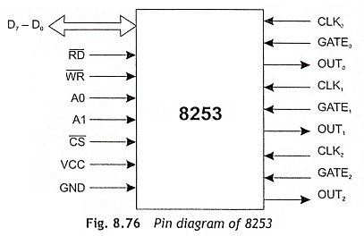
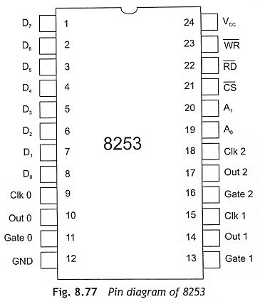
The programmer can program 8253 using software in any one of the six operating modes: Mode 0, Mode 1, Mode 2, Mode 3, Mode 4, and Mode 5. The pin diagram of 8253 Programmable Interval Timer is shown in Fig. 8.76 and Fig. 8.77. The functional descriptions of pins are as follows:
R̅D̅ (Read) When this pin is low, the CPU is inputting data in the counter.
W̅R̅ (Write) When this is low, the CPU is outputting data in the form of mode information or loading of counters.
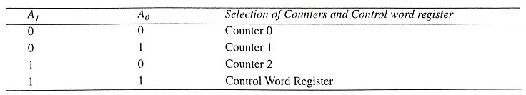
A0, A1 These pins are normally connected to the address bus. The function of these pins is used to select one of the three counters to be operated and to address the control word registers for mode selection as given below:
C̅S̅ Chip select A ‘low’ on C̅S̅ input enables the 8253. No reading or writing operation will be performed until the device is selected. The C̅S̅ input signal is not used to control the actual operation of the counters.
Data Bus Buffer The 3-state, bi-directional, 8-bit buffers exist in 8253. These buffers are used to interface the 8253 to the systems data bus D0-D7 lines. Data can be transmitted or received by the buffer upon execution of input and output CPU instructions. The data bus buffer has three basic functions, namely, programming the Modes of the 8253, loading the count registers and reading the count values.
D0-D7 Bi-directional Data Bus There are eight data lines through which the control word will be written in the control word register of 8253 counter/timer during programming. The counter will be written and read through the data bus.
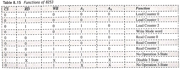
Read/Write Logic The read/write Logic accepts inputs from the system bus and in turn Gate generates control signals for operation of 8253. This is enabled by C̅S̅. Therefore, no operation can take place to change the function unless the device has been selected by the system logic. Table 8.15 shows the various functions of 8253 Programmable Interval Timer based on the status of pins associated with read/write logic.
CLK0, CLK1, CLK2 CLK0, CLK1 and CLK2 are clock for Counter 0, Counter 1 and Counter 2 respectively. The countdown of the counter takes place on each high to low transition of clock input.
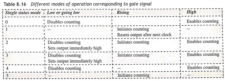
GATE0, GATE1, GATE2 GATE0, GATE1 and GATE2 are gate terminals of Counter 0, Counter 1 and Counter 2 respectively. The function of the GATE in different modes is illustrated in Table 8.16.
OUT0, OUT1, OUT2 OUT0, OUT1, OUT2 are output terminals of Counter 0, Counter 1 and Counter 2 respectively. The output of the 8253 timer depends Upon the mode of operation.
Block Diagram
The functional block diagram is illustrated in Fig. 8.75. This device can be divided into functional blocks such as the counter section and the CPU interface section.
Counter Section The 8253 consists of three programmable independent counters: Counter #0, Counter #1, and Counter #2. These three functional blocks of counters are identical in operation. Each counter consists of a single 16-bit down counter. The counter can operate in either binary or BCD and its input, gate and output are configured by the selection of modes stored in the Control Word Register. The counters are fully independent and each can have separate mode configuration and counting operation, binary or BCD. Each counter can be operated in any of six modes ( Mode 0 to Mode 5).
The reading of the contents of each counter is available to the programmer with simple READ operations for event counting applications. Special commands and logic are incorporated in the 8253 so that the contents of each counter can be read without having to inhibit the clock input.
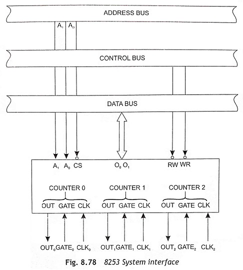
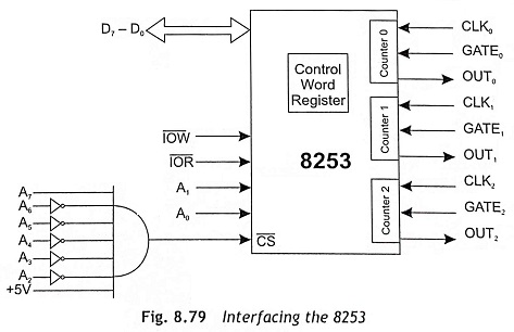
Systems Interface The C̅S̅ input signal enables the 8253 timer/counter IC. The R̅D̅ and W̅R̅ signals are used to read and write operation respectively. The 8253 can be interfaced with the microprocessor in the same manner as all other peripherals of the family. The 8253 8253 Programmable Interval timer/counter, which consists of three counters and the control register, will be treated by the systems software as an array of peripheral I/O ports for all modes of programming.
Figure 8.78 shows the interfacing between microprocessor and 8253 timer. The data bus D0-D7 is connected with the data bus of the microprocessor. The select inputs A0, A1 of 8253 connect to the A0, A1 address bus signals of the CPU. The C̅S̅ can be derived directly from the address bus using a linear select method or it can be connected to the output of a decoder.
Control Word Register
The systems software programs are all functions of the 8253. This device is programmed to initialize the counter, select the specified counter mode, and read the count value. A control word must be sent out by CPU to initialize each counter of the 8253 to operate in the desired mode. Before initialization, the mode count and output of all counters are undefined. The control words program the mode, loading sequence and selection of binary or BCD counting. Once programmed, the 8253 is ready to perform any operation which is assigned to carry out.
The control word register is selected when the pins A0 and A1 are 11. Then the control word register accepts information from the data bus buffer and stores it. The information stored in this register controls the operation of each counter. Each counter has three terminals: CLK, GATE and OUT. The output signal depends on the operating mode. The GATE signal controls the output signal.
All of the modes for each counter are programmed by a simple instruction. Writing a control word into the control word register individually programs each counter of the 8253. The control word format is shown below:
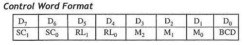
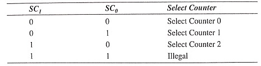
SC-Select Counter The SC0 and SC1 bits of the control word select a counter. The selection of counters is given below:
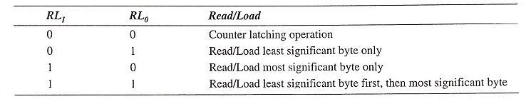
RL-Read/Load The RL0 and RL1 are used to load/read counts as follows:
M-Mode Mode selecting bits M0, M1 and M2 select any one of six modes as given below:
BCD
- 0 Binary counter (16 bits)
- 1 Binary coded decimal (BCD) counter (4 decades)
Reading While Counting The 8253 timer has an command for latching the content of a counter to read the count value without stopping the counting. This device has a special internal logic to achieve this. The count value can be read after loading a control word in the control word register. The bit pattern for the control word for this operation is as follows:
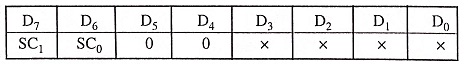
- SC1 and SC0-specify counter to be latched.
- D5 and D4-00 makes counter latching operation
- X-indicates ‘don’t care’.
For example, the control word for reading the count value of Counter 1 is
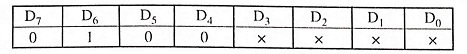
- Bits D7 and D6 are 0 and 1 respectively to represent Counter 1.
- Bits D5 and D4 are 0 and 0 to represent latching operation.
- Other bits are either 1 or 0.
Therefore, the control word for the above operation is 40H.
Whenever the microprocessor wants to latch the counter the latching command must be issued every time and then the content of counter read. In this mode of operation, counter operation will not be affected by the latching command. After receiving the latching command, the 8253 latches the content of the counter and stores it in a storage register. Then the microprocessor reads the content of the register by issuing a read instruction. This read operation is generally specified by RL1 and RL0 bits of the original mode set command. For counter latching operation, RL1 and RL0 are 0 and 0 respectively. If RL1 = 0 and RL0 = 1, only read least significant byte LSB of the counter. When RL1 = 1 and RL0 = 0, only read MSB of the count, If RL1 = 1 and RL0 = 1, read LSB of the count first, and thereafter read MSB of the count.
Operational Modes
The 8253 consists of three independent negative edge triggered 16-bit down counters, namely, Counter 0, Counter 1 and Counter 2. As the counters are fully independent, each counter of 8253 can be programmed in a different mode configuration and counting operation. The programmer must write the control word in the control word register and the load the count value in the selected count register. For writing the mode control word, the counter may be selected in any sequence. Each counter’s mode control word register has a separate address so that it can be loaded independently. Usually, the 8253 is available on a microprocessor kit. Sometimes 8253 Programmable Interval timer/counter is also connected with a Microprocessor kit externally. The clock frequency is about 1.5 MHz, which is available on the kit. If the clock frequency is about 3 MHz, an edge-triggered flip-flop can be used to divide this clock frequency by two to obtain a desired clock frequency for operating 8253 properly.
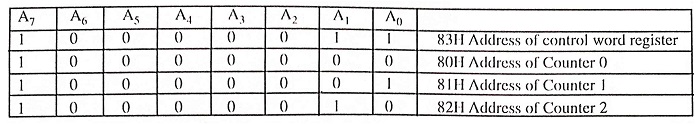
The port address for control word register and the counters of 8253 are as follows:
A counter can be used for various applications such as BCD/binary counter, programmable rate generator, square wave generator, hardware/software triggered strobe, programmable one-shot, to generate time delay, etc. Descriptions of some applications are given below.
MODE 0 Interrupt on Terminal Count Generally, Mode 0 is used to generate accurate time delay under software control. Firstly any one counter of 8253 timer/counter is initialized and loaded with a suitable count to develop the desired time delay. After termination of counting, the counter interrupts the microprocessor. When counter interrupts the microprocessor, the specified operations will be performed by the microprocessor. When the control word is loaded into the control word register, the 8253 Programmable Interval timer/counter sets the mode. In Mode 0 operation, the output of the counter becomes initially low after the mode is set. After mode set operation, the selected counter must be loaded by the desired count value N.
In this mode of operation, GATE is kept high. Therefore, just after loading the count registers, the counter starts to decrement. When counting is going on, the counter output terminal OUT remains low. As soon as the terminal count reaches 0, the output becomes high. The output remains high until the counter is reloaded or a new count value is loaded into the counter. When the count is reloaded or a new count is loaded, the counting restarts from new count value and again OUT becomes low. The timing diagram for Mode 0 operation is shown in Fig. 8.80.
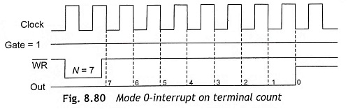
While counting is going on, GATE becomes low suddenly and the counter stops counting operation. After some time if the GATE returns to 1, counting is resumed from the count value at which the counting discontinued. The count value can be changed at any time. A new count value can also be loaded while counting is going on. But the changes will be effective only after the next GATE trigger. This mode of operation can be used to generate accurate time delay. This can also be used to perform specified operation after some delay. The output of OUT terminal may be used to interrupt the microprocessor.