8255A Programmable Peripheral Interface:
8255 is a programmable peripheral interface IC and is a multiport input/output device. This is a general-purpose programmable I/O device, which may be used with many different microprocessors. There are 24 I/O pins, which may be individually programmed in 2 groups of 12 and used, in 3 major modes of operation. The I/O ports can be programmed in a variety of ways as per requirement of the programmer. The features of 8255A Programmable Peripheral Interface device are given below:
Features of 8255A Programmable Peripheral Interface
- 24 programmable I/O pins
- Fully TTL compatible
- High speed, no ‘Wait State’ operation with 5 MHz 8085, 8 MHz 80C86 and 80C88
- Direct bit set/reset capability
- Enhanced control word read capability
- 2.5 mA drive capability on all I/O ports
- Low standby power static CMOS circuit design insures low operating power
Generally, this device is used to read data from an external device and write data into an external device. Some interface circuits are available for reading/writing data in an external device. These interface circuits are called peripheral interface circuits. These circuits are also known as programmable I/O ports as I/O ports are programmed to perform specified functions.
Architecture of Intel 8255A
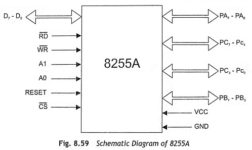
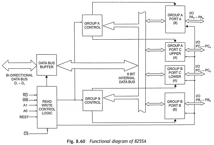
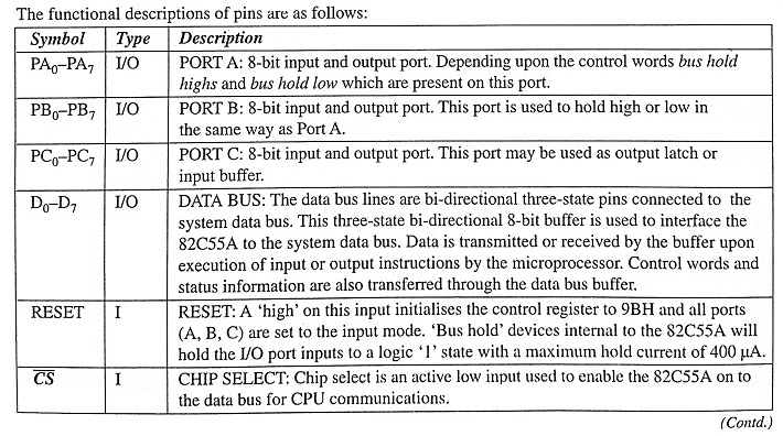
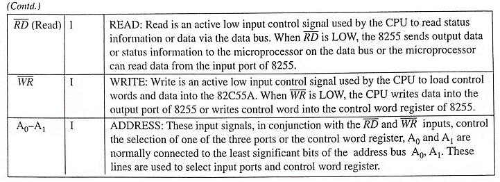
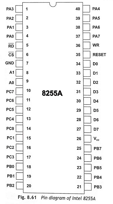
The schematic and pin diagrams of Intel 8255A Programmable Peripheral Interface are shown in Fig. 8.59 and Fig. 8.60 respectively. It is a 40-pin. IC package and operates on a single +5 V dc supply. The 8255A Programmable Peripheral Interface has 24 I/O pins, which may be individually programmed in two groups of twelve input/output lines or three groups of eight lines. The two groups of I/O pins are called Group A and Group B. Each group contains a subgroup of eight bits known as 8-bit port and a subgroup of four bits known as 4-bit port. This IC has three eight-bit ports: Port A (PA7-PA0), Port B (PB7-PB0), and Port C (PC7-PC0). Port C is divided into subgroups such as Port C upper, (PC7-PC4) and Port C lower, (PC3-PC0). Group A consists of Port A and Port C upper. Group B consists of Port B and Port C lower. The internal block diagram of 8255 is depicted in Fig. 8. 61. The pins for various ports are as follows:
PA0-PA7 are 8 pins of Port A, PB0-PB7 are 8 pins of Port B, PC0-PC3 are 4 pins of Port C lower and PC4-PC7 are 4 pins of Port C upper
Group A and Group B Controls
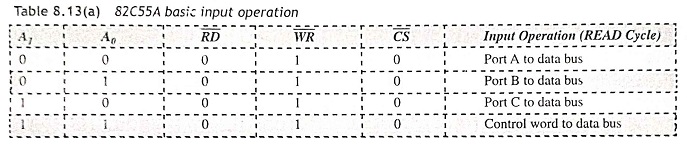
The functional configuration of each port can be programmed by the instruction. For this, the CPU stores a control word to the 82C55A. The control word contains information about the mode of operation, bit set, bit reset. etc. The control word initializes the functional configuration of the 82C55A. Each of the control blocks, Group A and Group B, receive ‘commands’ from the control logic signals: R̅D̅ and W̅R̅ receive ‘control words’ from the internal data bus and issue the proper commands to their associated ports.
- Control Group A-Port A and Port C upper (PC7-PC4)
- Control Group B-Port B and Port C lower (PC3-PC0)
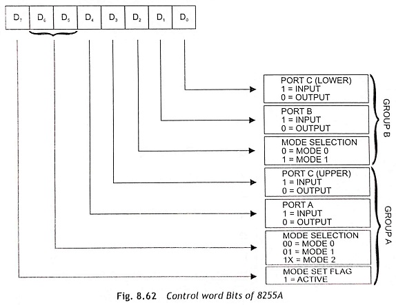
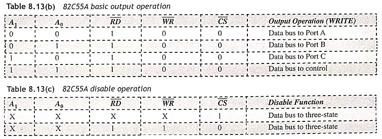
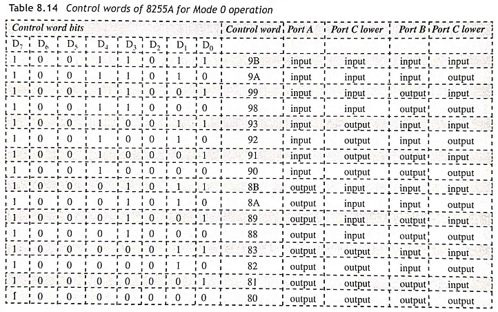
The control word register can be both written and read as shown in the ‘Basic Operation’ Table 8.13. The control word format for both read and write operations is depicted in Fig. 8.62. When the control word is read, the bit D7 will always be a logic ‘1’, as this implies control-word mode information.
Operating Modes
There are three basic modes of operation of 8255 as follows:
- Mode 0-Basic input/output
- Mode 1-Strobed input/output
- Mode 2-Bi-directional bus
The system software can select the mode of operation. When the reset input becomes `high’, all ports will be set to the input mode with all 24-port lines held at logic ‘one’ level by internal bus hold devices. When the reset is removed, the 82C55A can remain in the input mode with no additional initialization required. This eliminates the need to pull up or pull down resistors in all CMOS designs. Then the control word register will contain 9B H. During the execution of the system program, any of the other modes may be selected using a single output instruction. This allows a single 82C55A to service a variety of peripheral devices with a simple software maintenance routine. Any port programmed as an output port is initialized to all zeros when the control word is written.
The 8255A Programmable Peripheral Interface has two 8-bit ports (Port A and Port B) and two 4-bit ports (Port C upper and Port C lower). The modes for Port A and Port B can he separately defined, though Port C is divided into two portions as required by the Group A and Group B definitions.
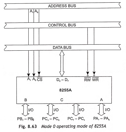
Mode 0-Basic input/Output This functional configuration provides simple input and output operations for each of the three ports. Each of the four ports of 8255 can he programmed to be either an input or output port. No handshaking is required; data is simply written to or read from a specific port.
Basic functional definitions of Mode 0 are as follows:
- Two 8-bit ports and two 4-bit ports
- Any port can be input or output
- Outputs are latched
- Inputs are not latched
- 16 different input/output configurations possible
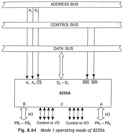
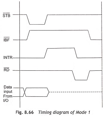
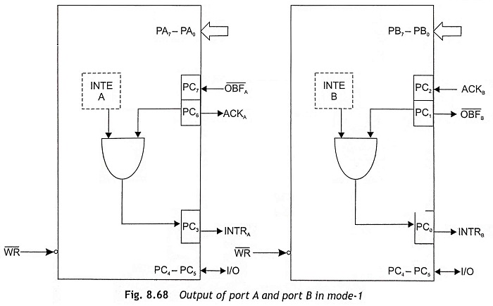
Mode 1-Strobed Input/Output This is strobed input/output mode of operation. Only Port A and Port B both can be operating in this mode of operation. When Port A and Port B are programmed in Mode 1, six pins from Port C are used as control signals. These control signals are used for handshaking. PC0, PC1 and PC2 pins of PC lower are used to control Port B and PC3, PC4, and PC5 pins of PC upper are used to control Port A. The other pins of Port C, i.e., PC6 and PC7 can be used as either input or output. While Port A From is operated as an output port, pins PC3, PC6 and PC7 are used for its control. The pins PC4 and PC5 can be used either as input or output. The combination of Mode 0 and Mode 1 operation is also possible. When Port A is programmed to operate in Mode 1, Port B can also be operated in Mode 0. Figure 8.66 shows the timing diagram of Mode 1(input).
This functional configuration provides a means for transferring I/O data to or from a specified port in conjunction with strobes or handshaking signals. In Mode 1, Port A and Port B use the lines on Port C to generate or accept these handshaking signals. In Mode 1, the 8255A Programmable Peripheral Interface has two functional groups, namely, Group A and Group B. Each group contains one 8-bit port and a 4-bit control/data port. The 8-bit data port can be either input or output. Both inputs and outputs are latched. The 4-bit port can be used for control and status of the 8-bit port. Figure 8.67 shows the Mode 1 operation of Port A and Port B as input ports. Figure 8.68 shows the Mode 1 operation of Port A and Port B as output ports.
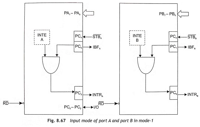
Input Control Signals
STB (Strobe Input) A low on this input loads data into the input latch.
IBF (Input Buffer Full F/F) A high on this output indicates that the data has been loaded into the input latch: in essence, and acknowledgment. IBF is set by S̅T̅B̅ input being low and is reset by the rising edge of the R̅D̅ input.
INTR (Interrupt Request) A ‘high’ on this output can be used to interrupt the CPU when an input device is requesting service. INTR is set by the conditions: S̅T̅B̅ is a ‘one’, IBF is a ‘one’ and INTE is a ‘one’. It is reset by the falling edge of R̅D̅. This procedure allows an input device to request service from the CPU by simply strobing its data into the port.
INTE A Controlled by bit set/reset of PC4.
INTE B Controlled by bit set/reset of PC2.
Output Control Signals
O̅B̅F̅ (Output Buffer Full F/F) The O̅B̅F̅ output will go ‘low’ to indicate that the CPU has written data out to be specified port. This does not mean valid data is sent out of the part at this time since O̅B̅F̅ can go true before data is available. Data is guaranteed valid at the rising edge of O̅B̅F̅. The O̅B̅F̅ F/F will be set by the rising edge of the W̅R̅ input and reset by A̅C̅K̅ input being low.
A̅C̅K̅ (Acknowledge Input) A ‘low’ on this input informs the 82C55A that the data from Port A or Port B is ready to be accepted. In essence, a response from the peripheral device indicates that it is ready to accept data.
INTR (Interrupt Request) A ‘high’ on this output can be used to interrupt the CPU when an output device has been accepted by data transmitted by the CPU. INTR is set when A̅C̅K̅ is a ‘one’, OBF is a ‘one’ and INTE is a ‘one’. It is reset by the falling edge of W̅R̅.
INTE A Controlled by bit set/reset of PC6.
INTE B Controlled by bit set/reset of PC2.
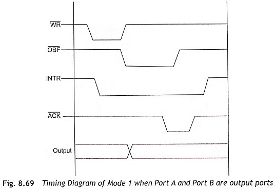
The strobe line is in a handshaking mode. The user needs to send O̅B̅F̅ to the peripheral device, generate an A̅C̅K̅ from the peripheral device and then latch data into the peripheral device on the rising edge of O̅B̅F̅. The timing diagram of 8255 in Mode 1 operation of Port A and Port B as output port is illustrated in Fig. 8.69.
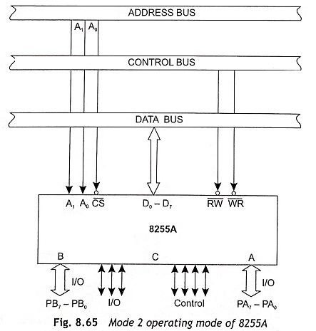
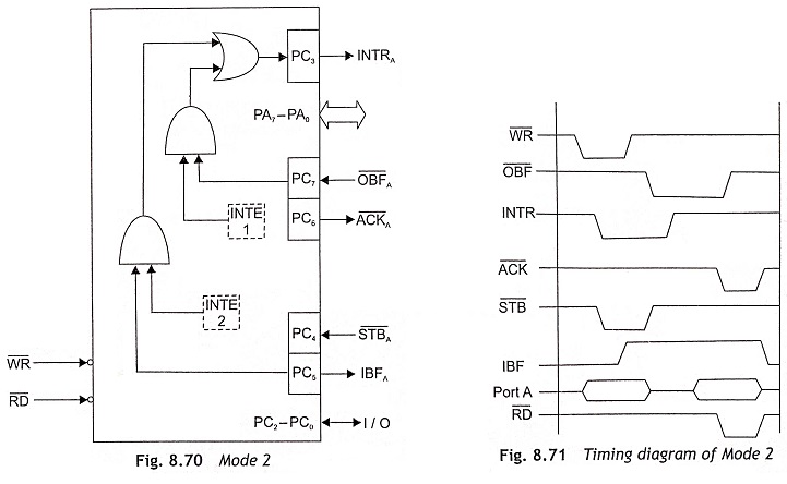
Mode 2-Bi-directional Bus This mode is strobed bi-directional of operation of port with input and output capability. Mode 2 operation is only feasible for Port A. Therefore, Port A can be programmed to operate as a bi-directional port. If Port A is programmed in Mode 2, Port B can be used in either Mode 1 or Mode 0. In this mode of operation, PC3 to PC7 pins are used to control signals of Port A.
The basic functional definitions of Mode 2 are
- Used in Group A only
- One 8-bit, bi-directional bus port (Port A) and a 5-bit control port (Port C)
- Both inputs and outputs are latched
- The 5-bit control port (Port C) is used for control and status for the 8-bit, bi-directional bus port (Port A)
Bi–Directional Bus I/O Control Signal
- INTR – (Interrupt Request) A high on this output can be used to interrupt the CPU for both input or output operations.
Output Operations
- OBF (Output Buffer Full) The OBF output will go ‘low’ to indicate that the CPU has written data out to Port A.
- ACK (Acknowledge) A ‘low’ on this input enables the three-state output buffer of Port A to send out the data. Otherwise, the output buffer will be in the high-impedance state.
- INTE 1 (The INTE flip-flop associated with OBF) Controlled by bit set/reset of PC4.
Input Operations
- STB (Strobe Input) A ‘low’ on this input loads data into the input latch.
- IBF (Input Buffer Full F/F) A ‘high’ on this output indicates that data has been loaded into the input latch.
- INTE 2 (The INTE Flip-Flop associated with IBF) Controlled by bit set/reset of PC4. The timing diagram of Mode 2 operation of 8255 is depicted in Fig. 8.71.
Single-Bit Set/Reset (BSR) Mode
In this mode, any of the eight bits of Port C can be set or reset using a single output instruction. This feature reduces software requirements in control-based applications.
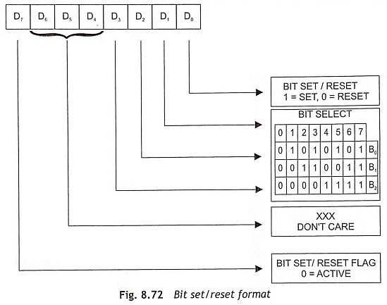
When Port C is being used as status/control for Port A or B, these bits can be set or reset by using the bit set/reset operation just as if they were output ports. Figure 8.72 shows the bit set/reset format.
Control Word
The ports of 8255A can be operating any one mode by programming the internal register of 8255A. This internal register of 8255 PPI is known as Control Word Register (CWR). To program the ports of 8255, a control word is formed. Figure 8.72 shows the bits of the control word. Only write operation of the control word register is permissible and no read operation of the control word register is allowed. Writing the control word into control word register, the IC will be configured to operate specified modes of operation. The functional description of the bits of the control word is as follows:
- Bit No. D0 The D0 bit is used to set Port C lower. When this bit is set to 1, Port C lower is an input port. If the bit is set to 0, Port C lower is an output port.
- Bit No. D1 This bit is used for Port B. When this bit is set to 1, Port B is an input port. If the bit is set to 0, Port B is an output port.
- Bit No. D2 The bit D2 is used for the selection of the mode operation of Port B. If this bit is set to 0, Port B can be operating in Mode 0. For Mode 1 operation, D2 is set 1.
- Bit No. D3 It is used for the Port C upper If the bit is set to 1, Port C upper is an input port. When the bit is set to 0, Port C upper is an output port.
- Bit No. D4 The bit D4 sets Port A for input or output operation. When this bit is 1, Port A can be used as input port. When it is 0, Port A becomes output port.
- Bit No. D5 and D6 These bits are used to select the operating mode of Port A, for Port A can be operate in Mode 0, Mode 1 and Mode 2. The mode of operation is selected by D5 and D6 as given below:
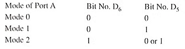
For Mode 2, bit No. 5 is set to either 0 or 1; it is immaterial.
- Bit No. D7 This bit selects the I/O mode or bit set/reset mode. When it is 1 ports A, B and C are defined as input/output port. If it is set to 0, bit set/reset mode is selected.
Applications of 8255 PPI
The 8255 PPI IC is a very powerful tool for interfacing peripheral equipment to the microprocessor-based system. It represents the optimum use of available pins and is flexible enough to interface almost any I/O device without the need for additional external logic.
Each peripheral device in a microprocessor-based system usually has a ‘service routine’ associated with it. The routine manages the software interface between the device and the microprocessor. The functional definition of the 8255 can be programmed by the I/O service routine and becomes an extension of the system software. By examining the I/O device interface characteristics for both data transfer and timing, and matching this information to the examples and tables in the detailed operational description, a control word must be developed and loaded into control word register to initialize the 8255 IC to get a specified operation. The typical applications of the 8255 are given below:
- Putting on LED as specified by the designer
- Generating a square wave at Port A
- Interfacing A/D converter
- Keyboard operation
- Sequential switching of lights
- Traffic light control
- Interfacing with dc motors and stepper motors