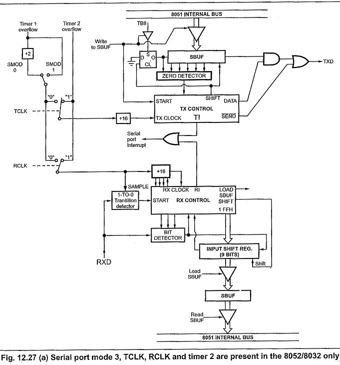
Serial Communication Interface in Microprocessor:
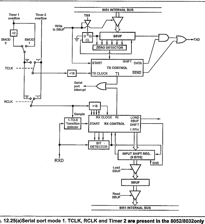
The Serial Communication Interface in Microprocessor is full duplex, meaning it can transmit and receive simultaneously. It is also receive-buffered, meaning it can commence reception of a second byte before a previously received byte has been read from the receive register. (However, if the first byte still hasn’t been read by the time reception of the second byte is complete, one of the bytes will be lost). The serial port receive and transmit registers are both accessed at Special Function Register SBUF. Writing to SBUF loads the transmit register, and reading SBUF accesses a physically separate receive register.
Operating Modes for Serial Port MODE 0
In this mode, Serial Communication Interface in Microprocessor data enters and exits through RXD. TXD outputs the shift clock. 8 bits are transmitted/received : 8 data bits (LSB first). The baud rate is fixed at 1/12 the oscillator frequency.
MODE 1
In this mode, 10 bits are transmitted (through TXD) or received (through RXD) : a start bit (0), 8 data bits (LSB first), and a stop bit (1). On receive, the stop bit goes into RB8 in Special Function Register SCON. The baud rate is variable.
MODE 2
In this mode, 11 bits are transmitted (thorugh TXD) or received (through RXD) : a start bit (0), 8 data bits (LSB first), a programmable 9th data bit, and a stop bit (1). On Transmit, the 9th data bit (TB8 in SCON) can be assigned the value of 0 or 1. Or, for example, the parity bit (P, in the PSW) could be moved into TB8. On receive, the 9th data bit goes into RB8 in Special Function Register SCON, while the stop bit is ignored. The baud rate is programmable to either Y32 or 14 the oscillator frequency.
MODE 3
In this mode, 11 bits are transmitted (through TXD) or received (through RXD) : a start bit (0), 8 data bits (LSB first), a programmable 9th data bit and a stop bit (1). In fact, Mode 3 is the same as Mode 2 in all respects except the baud rate. The baud rate in Mode 3 is variable.
In all four modes, transmission is initiated by any instruction that uses SBUF as a destination register. Reception is initiated in Mode 0 by the condition RI = 0 and REN = 1. Reception is initiated in the other modes by the incoming start bit if REN = 1.
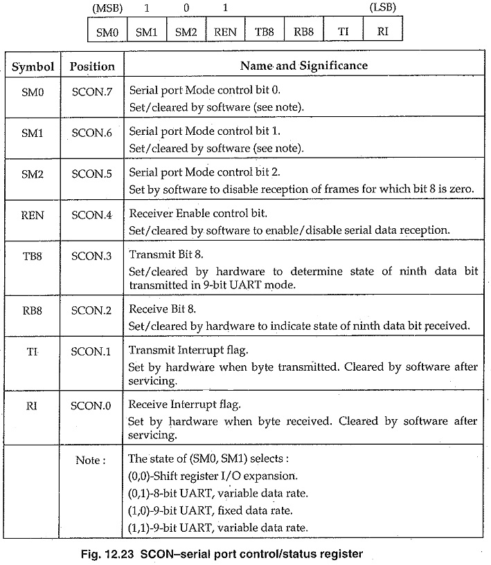
Serial Port Control Register
The serial port control and status regsiter is the Special Function Register SCON, shown in Fig. 12.23. This register contains not only the mode selection bits, but also the 9th data bit for transmit and receive (TB8 and RB8), and the Serial Communication Interface in Microprocessor port interrupt bits (TI and RI).
Generating Baud Rates
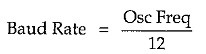
Serial Port in Mode 0 :
Mode 0 has a fixed baud rate which is 1/12 of the oscillator frequency. To run the Serial Communication Interface in Microprocessor port in this mode none of the Timer/Counters need to be set up. Only the SCON register needs to be defined.
Serial port in Mode 1
Model has a variable baud rate. The baud rate can be generated by either Timer 1 or Timer 2 (8052 only).
Using Timer/Counter 1 to Generate Baud Rates
For this purpose, Timer 1 is used in mode 2 (Auto-Reload).
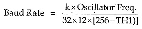
If SMOD = 0, then K = 1.
If SMOD = 1, then K = 2. (SMOD is the PCON register)
Most of the time the user knows the baud rate and needs to know the reload value for TH1. Therefore, the equation to calculate TH1 can be written as :
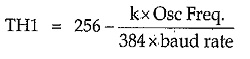
TH1 must be an integer value. Rounding off TH1 to the nearest integer may :not produce the desired baud rate. In this case, the user may have to choose another crystal frequency.
Since the PCON register is not bit addressable, one way to set the bit is logical ORing the PCON register.
Using Timer/Counter 2 to Generate Baud Rates
For this purpose, Timer 2 must be used in the baud rate generating mode. If Timer 2 is being clocked through pin T2 (P1.0) the baud rate is :
![]()
And if it is being clocked internally the baud rate is :
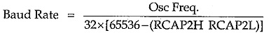
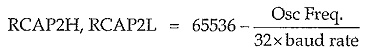
To obtain the reload value for RCAP2H and RECAP2L the above equation can be rewritten as
Serial Port in Mode 2
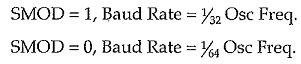
The baud rate is fixed in this mode and is 1/32 or 1/64 of the oscillator frequency depending on the value of the SMOD bit in the PCON register. In this mode none of the Timers are used and the clock comes from the internal phase 2 clock.
To set the SMOD bit : ORL PCON, #80H. The address of PCON is 87H.
Serial Port in Mode 3
The baud rate in mode 3 is variable and sets up exactly the same as in mode
More About Mode 0
Serial data enters and exits through RXD, TXD outputs the shift clock. 8 bits are transmitted /received : 8 data bits (LSB first). The baud rate is fixed at 1/12 the oscillator frequency.
Fig. 12.24 shows a simplified functional diagram of the Serial Communication Interface in Microprocessor in Mode 0, and associated timing. Transmission is initiated by any instruction that uses SBUF as a destination register. The “write to SBUF” signal at S6P2 also loads a 1 into the 9th position of the transmit shift register and tells the TX control block to commence a transmission. The internal timing is such that one full machine cycle will elapse between “write to SBUF,” and activation of SEND.
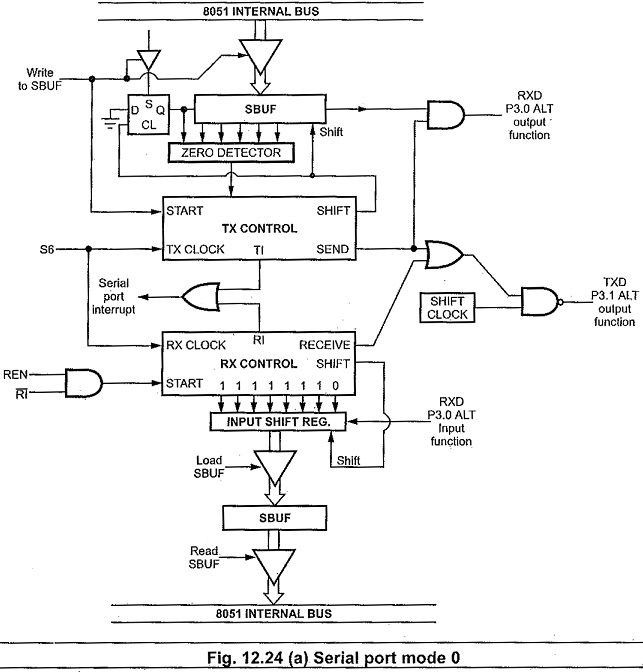
SEND enables the output of the shift- register to the alternate output function line of P3.0, and also enables SHIFT CLOCK to the alternate output function line of P3.1. SHIFT CLOCK i s low during S3, S4 and S5 of every machine cycle, and high during S6, S1 and S2. At S6P2 of every machine cycle in which SEND is active, the contents of the transmit shift register are shifted to the right one position.
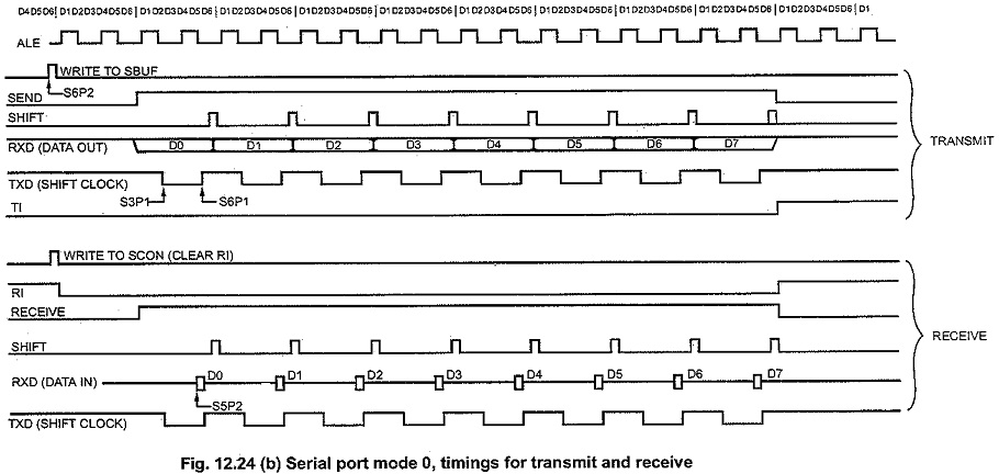
As data bits shift out to the right, zeroes come in from the left. When the MSB of the data byte is at the output position of the shift register, then the 1 that was initially loaded, into the 9th position, is just to the left of the MSB and all positions to the left of that contain zeros. This condition flags the TX Control block to do one last shift and then deactivate SEND and set Both of these actions occur at S1P1 of the 10th machine cycle after “write to SBUF.”
Reception is initiated by the condition REN =1 and R1= 0. At S6P2 of the next machine cycle, the RX Control unit writes the bits 11111110 to the receive shift register, and in the next clock phase activates RECEIVE.
RECEIVE enables SHIFT CLOCK to the alternate output function line of P3.1. SHIFT CLOCK makes transitions at S3P1 and S6P1 of every machine cycle. At S6P2 of every machine cycle in which RECEIVE is active, the contents of the receive shift regsiter are shifted to the left one position. The value that comes in from the right is the value that was sampled at the P3.0 pin at S5P2 of the same machine cycle.
As data bits come in from the right, is shift out to the left. When the 0 that was initially loaded into the right most position arrives at the leftmost position in the shift register, it flags the RX control block to do one last shift and load SBUF. At S1P1 of the 10th machine cycle after the write to SCON that cleared RI, RECEIVE is cleared and RI is set.
More About Mode 1
Ten bits are transmitted (through TXD), or received (through RXD) : a start bit (0), 8 data bits (LSB first), and a stop bit (1). On receive, the stop bit goes into RB8 in SCON. In the 8051 the baud rate is determined by the Timer 1 overflow rate. In the 8052 it is determined either by the Timer 1 overflow rate, or the Timer 2 overflow rate, or both (one for transmit and the other for receive).
Fig. 12.25 shows a simplified functional diagram of the serial port in Mode 1, and associated timings for transmit receive.
Transmission is initiated by any instruction that uses SBUF as a destination register. The “write to SBUF” signal also loads a 1 into the 9th bit position of the transmit shift register and indicates the TX Control unit that a transmission is requested. Transmission actually commences at S1P1 of the machine cycle following the next rollover in the divide-by-16 counter. (Thus, the bit times are synchronized to the divide-by-16 counter, not to the “write to SBUF” signal).
The transmission begins with activation of SEND, which puts the start bit at TXD. One bit time later, DATA is activated, which enables the output bit of the transmit shift regsiter to TXD. The first shift pulse occurs one bit time after that.
As data bits shift out to the right, zeroes are clocked in from the left. When the MSB of the data byte is at the output position of the shift regsiter, the 1 that was initially loaded . into the 9th position is just to the left of the MSB, and all positions to the left of that contain zeroes. This condition indicates the TX Control unit to do one last shift and then deactivate SEND and set TI. This occurs at the 10th divide-by-16 rollover after “write to SBUF.”
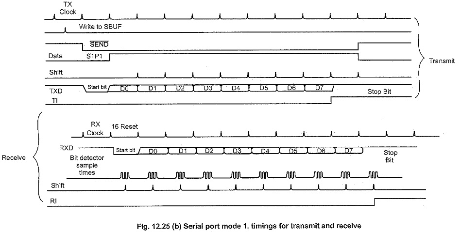
Reception is initiated by a detected 1 to 0 transition at RXD. For this purpose RXD is sampled at a rate of 16 times whatever baud rate has been established. When a transition is detected, the divide by 16 counter is immediately reset, and 1FFH is written into the input shift register. Resetting the divide by 16 counter aligns its rollovers with the boundaries of the incoming bit times.
The 16 states of the counter divide each bit time into 16ths. At the 7th, 8th and 9th counter states of each bit time, the bit detector samples the value of RXD. The value accepted is the value that was seen in at least 2 of the 3 samples. This is done for noise rejection. If the value accepted during the first bit time is not 0, the receive circuits are reset and the unit goes back to looking for another 1 to 0 transition. This is to provide rejection of false start bits. If the start bit proves valid, it is shifted into the input shift register, and reception of the rest of the frame will proceed.
As data bits come in from the right, 1s shift out to the left. When the start bit arrives at the leftmost position in the shift register, (which in mode 1 is a 9-bit register), it indicates the RX control block to do one last shift, load SBUF and RB8 and set RI. The signal to load SBUF and RB8 and to set RI, will be generated if, and only if, the following conditions are met at the time the final shift pulse is generated.
-
RI = 0 and
-
Either SM2 = 0, or the received stop bit = 1
If either of these two conditions is not met, the received frame is irretrievably lost. If both conditions are met, the stop bit goes into RB8, the 8 data bits go into SBUF, and RI is activated. At this time, whether the above conditions are met or not, the unit goes back to looking for a 1 to 0 transition in RXD.
More About Modes 2 and 3
Eleven bits are transmitted (through TXD), or received (through RXD) : a start bit (0), 8 data bits (LSB first), a programmble 9th data bit, and a stop bit (1). On transmit, the 9th data bit (TB8) can be assigned the value of 0 to 1. On receive, the 9th data bit goes into RB8 in SCON. The baud rate is programmable to either 1/32 or 1/64 the oscillator frequency in Mode 2. Mode 3 may have a variable baud rate generated from either Timer 1 or 2 depending on the state of TCLK and RCLK.
Fig. 12.26 and 12.27 show a functional diagram of the Serial Communication Interface in Microprocessor port in Modes 2 and 3. The receive portion is exactly the same as in Mode 1. The transmit portion differs from Mode 1 only in the 9th bit of the transmit shift register.
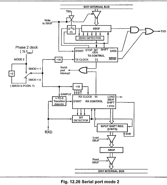
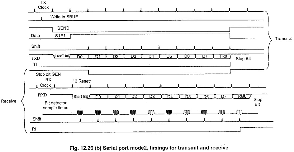
Transmission is initiated by any instruction that uses SBUF as a destination register. The “write to SBUF” signal also loads TB8 into the 9th bit position of the transmit shift register and indicates the TX control unit that a transmission is requested. Transmission commences at S1P1 of the machine cycle following the next rollover in the divide-by-16 counter. (Thus, the bit times are synchronized to the divide-by-16 counter, not to the “write to SBUF” signal.)
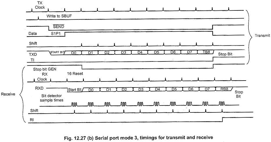
The transmission begins with activation of SEND, which puts the start bit at TXD. One bit time later, DATA is activated, which enables the output bit of the transmit shift register to TXD. The first shift pulse occurs one bit time after that. The first shfit clocks a 1 (the stop bit) into the 9th bit position of the Shift registers. Thereafter, only zeroes are clocked in.
Thus, as data bits shift out to the right, zeroes are clocked in from the-left. When TB8 is at the output position of the shift register, the stop bit is just to the left of TB8, and all positions to the left of that contain zeroes. This condition indicates the TX Control unit to do one last shift and then deactivate SEND and set TI. This occurs at the 11th divide by 16 rollover after “write to SBUF.”
Reception is initiated by a detected 1 to 0 transition at RXD. For this purpose RXD is sampled at a rate of 16 times whatever baud rate has been established. When a transition is detected, the divide by 16 counter is immediately reset and 1FFH is written to the input shift register.
At the 7th, 8th and 9th counter states of each bit time, the bit detector samples the value of RXD. The value accepted is the value that was seen in at least 2 of the 3 samples. If the value accepted during the first bit time is not 0, the receive circuits are reset and the unit goes back to looking for another 1 to 0 transition. If the start bit proves alied, it is shifted into the input shift register, and reception of the rest of the frame will proceed.
As data bits come in from the right, is shift out to the left. When the start bit arrives at the leftmost pOsition in the shift register (Which in Modes 2 and 3 is a 9-bit register), it flags the RX control block to do one last shift, load SBUF and RB8 and set RI. The signal to load SBUF and RB8 and to set RI, will be generated if, and only if, the following conditions are met at the time the final shift pulse is generated :
-
R1 = 0 and
-
Either SM2 = 0 or the received 9th data bit = 1
If either of these conditions is not met, the received frame is irretrievably lost, and RI is not set. If both conditions are met, the received 9th data bit goes into RB8, and the first 8 data bits go into SBUF. One bit time later, whether the above conditions were met or not, the unit goes back to looking for a 1 to 0 transition at the RXD input.
Note that the value of the received stop bit is irrelevant to SBUF, RB8 or RI.