Bus Interface in Microprocessor:
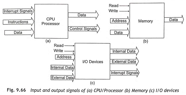
Bus Interface in Microprocessor – A microcomputer consists of a set of components such as CPU, memory, I/O device and these components communicate with each other to perform a specified task. The collection of paths which connect the various devices or modules is called the interconnection structure. The design of the interconnection structure depends on the exchange of data between different devices or modules as shown in Figure 9.66.
There are different types of data transfer such as
- Memory devices to CPU
- CPU to memory devices
- I/O devices to CPU
- CPU to I/O devices
- I/O devices to or from memory
System Bus
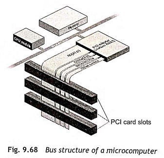
A bus is a communication pathway which can connect two or more devices (CPU, memory and I/O). Actually, the bus is a set of circuits that runs throughout the board and connects all the expansion slots, memory, I/O devices and CPU together. The characteristic of a bus is that it is a shared transmission medium. A bus consists of multiple pathways or lines. Each line is capable to transmit digital signal representing a binary digit, either 1 or 0. A sequence of bits can be transmitted across a single line. Simultaneously, several lines can be used to transmit bits in parallel. A bus that connects major components such as the CPU, memory, and I/O is called system bus. The most commonly used microcomputer interconnection structures is shown in Fig. 9.67 and 9.68.
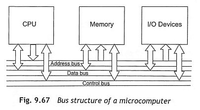
A system bus consists of 50-100 lines. Each line is assigned a particular function. The bus lines are classified into 3 groups such as data bus, address bus and control bus.
The data bus provides a path for moving data between the system modules or devices. These lines are also called data lines. The data bus typically consists of 8,16 or 32 separate lines, actually the numbers of lines being transferred to as the width of the data bus. Each line is capable of carrying only 1 bit at a time and the number of lines determines how many bits can be transferred at a time to increase overall system performance.
The address bus is used to locate the source or destination of the data on the data bus. The width of the address bus determines the maximum possible memory capacity of the system. The address bus is also known as address lines.
The control bus is used to control the access to and the use of the data and address lines. The most commonly used control lines are memory read, memory write, I/O read, I/O write, clock, reset, bus request, bus grant, interrupt request, interrupt acknowledge (ACK) and transfer ACK.
The operation of the bus is to transfer data from one device to other device via the buses. In a physical bus architecture, the system bus is a number of parallel electrical conductors. The conductors are metal lines etched in a card or printed circuit board. The bus extends across all of the components to connect with the bus lines.
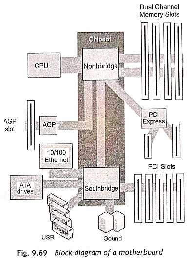
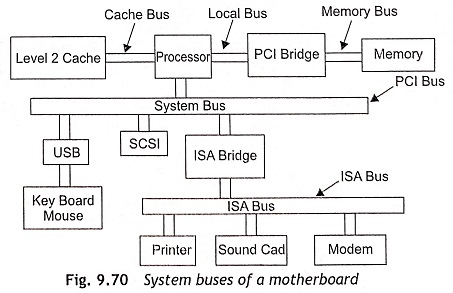
Generally, the motherboard of a microcomputer is the physical arrangement of a computer, which consists of all the computer’s components such as CPU/microprocessor, co-processors, memory, BIOS, expansion slots and interconnecting circuitry. Some additional components can be added to a motherboard through its expansion slots. The electronic interface between the motherboard and the smaller cards in the expansion slots is also called the bus. The personal computer consists of several types of buses on the motherboard as shown in Fig. 9.69, and the block diagram representation of a typical motherboard is depicted in Fig. 9.70. Most commonly used buses are
□ CPU bus or system bus
□ Cache bus
□ Memory bus
□ I/O or Expansion Bus:
- ISA (Industry Standard Architecture)
- EISA (Extended ISA)
- MCA (Micro Channel Architecture)
- PCI Bus (Peripheral Connection Interface)
- VL Bus (VESA Local Bus)
□ External Buses which are used to connect devices through external cables
- SCSI Bus
- PC Card Bus
- USB Bus
BUS Architecture
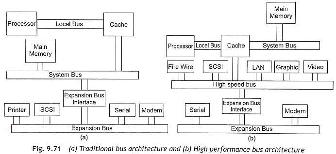
In multiple bus architecture, two or more devices are attached to the system bus, and propagation delays affect the performance of computer system. But the aggregate data transfer of the system bus is limited, and it is a bottleneck for data transfer as graphics and video controller. Therefore, buses are increased and they are interconnected in a certain configuration. The multiple bus architectures are classified as traditional bus architecture and high performance bus architecture. The traditional bus architecture has local bus between CPU and cache, system bus between main memory and cache, and expansion bus between I/O modules and main memory as shown in Figure 9.71. Figure 9.71(b) shows the high-performance bus architecture which consists of local bus between CPU and cache/bridge, system bus between cache/bridge and memory, high speed bus between high speed I/O devices and cache, and expansion bus between low speed I/O devices and expansion interface.
CPU or Processor Bus The CPU bus is the highest-level bus through which the chipset uses to send information to the processor and receive information from the processor.
Cache Bus In high-level bus architecture, the Pentium processors use a dedicated bus for accessing the system cache. This is also known as backside bus. In motherboards, the cache is connected to the standard memory through the cache bus.
Memory Bus The memory bus is a second-level system bus which connects the memory subsystem to the processor. In some systems, the processor bus is used as memory bus.
Local I/O Bus This bus is a high-speed input/output bus used for connecting peripherals to the memory, I/O devices and processor. For example, audio cards, video cards, disk storage devices, high-speed networks interfaces generally use the local I/O bus of this sort. The most commonly used local I/O buses are the VESA Local Bus (VLB) and the Peripheral Component interconnect Bus (PCI).
Standard I/O Bus The standard I/O buses are used for slower peripherals such as mice, modems, regular sound cards and low-speed networking. Nowadays, in all modern PCs, this is used as the Industry Standard Architecture (ISA) bus.
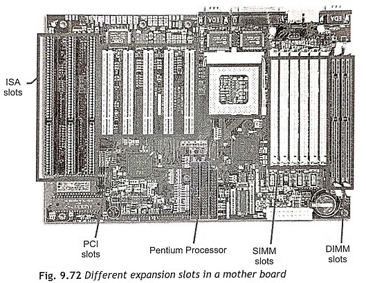
Expansion Bus All the above buses are located on the motherboard of a computer. In the motherboard of all personal computers, expansion slots are available to add cards or boards for more memory, graphics capabilities, and support for special devices. The boards inserted into the expansion slots are called expansion boards, expansion cards, and add-on-cards. On each slot, we can insert expansion boards such as soundcards, graphics cards, TV cards, etc., to create additional facility to the personal computer. Actually, these boards can communicate with the other hardware devices in the system. There are different ‘slots’ on the motherboard as shown in Fig. 9.72 and the names of the slots are as follows:
- ISA — Industry Standard Architecture
- EISA — Extended ISA
- MCA — Micro-Channel Architecture
- VESA — Video Electronics Standards Association
- PCI — Personal Component Interconnect
- AGP — Accelerated Graphics Port
- SIMM — Single Inline Memory Module
- DIMM — Dual Inline Memory Module
- PCMCIA— Personal Computer Memory Card International Association
In this section, ISA, EISA, MCA, VESA, PCI, and AGP are discussed elaborately.
ISA (Industry Standard Architecture)
The ISA stands for Industry Standard Architecture and it is pronounced as ‘eye-es-ch’. This bus architecture was developed by IBM in 1979. Actually, this bus was introduced in the IBM PC XT in 1981 as an 8 bit expansion slot and this bus operates at 8.3 MHz with a data rate of 7.9 Mbytes/s. After that 16-bit ISA bus introduced in the IBM PC AT machines in 1984 and runs at 15.9 MHz, with data rate of 15.9 Mbytes/s. This bus is called AT bus and presently all ISA slots are 16-bits. The ISA allows 16 bits of information at a time to flow between the motherboard circuit and an expansion slot card and its associated devices.
EISA (Extended Industry Standard Architecture)
EISA is a standard bus architecture that extends the ISA standard to a 32-bit interface. It was developed by IBM competotors such as HP, AST, Compaq, and Epson, etc., in 1987 and it was used as an alternative of the Micro Channel Architecture (MCA). EISA is hardware compatible with ISA. EISA data transfer can run at 33 Megabytes per second.
MCA (Micro Channel Architecture)
The Micro Channel Architecture was introduced by IBM in 1987 and used in PS/2 desktop computers. The MCA can be used as an interface between computers and their expansion cards and associated devices.
The pin connections in MCA are smaller than other bus interfaces. Therefore, MCA does not support other bus architectures.
VESA (Video Electronics Standards Association)
VESA stands for video electronics standards association. This bus is also called VL-Bus or VESA Local Bus (VLB). VESA Local Bus was developed in 1990 and supports 32-bit data flow at speeds of up to 40 MHz. VESA VL bus is a standard interface between a computer and its expansion slot. This bus provides faster data flow between the peripheral devices (video, disk, network) controlled by the expansion cards and microprocessor. This bus is a ‘local bus’ and it provides a physical path on which data flows at the speed of the microprocessor. The VESA local bus architecture was very popular on 80486 based computer systems in 1993 and 1994. The advantages of VESA bus are as follows:
- Faster processing
- 32-bit data-transfer capability
- Direct access to the processor bus, which is local to the CPU
- Direct access to system memory at the speed of the processor
- Faster access
- Different physical slot that prevents plugging a slower card into a fast slot
- 128 MBps to 132 MBps maximum throughput
The limitations of VESA bus are
- Available only for 80486 processors
- Maximum speed of the VESA specification is 66 MHz, though it’s speed is limited to 33 MHz
- Poor implementation of bus mastering
- This bus do not support plug-and-play
- VESA bus cannot be used for the speed of the Pentium
- Limited to a maximum of three cards depending on system resources
PCI (Peripheral Component Interconnect)
PCI (Peripheral Component Interconnect) bus was developed by Intel in 1993, ISA has been replaced by the PCI local bus architecture. These are the smaller and white-colored slots on the motherboard. PCI is a 64-bit bus, but it is usually implemented as a 32-bit bus. This bus runs at clock speeds of 33 MHz or 66 MHz. At 32 bits and 33 MHz, the data transfer rate is 133 MBps.
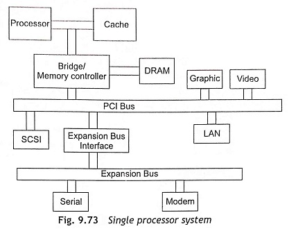
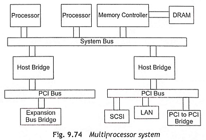
PCI is an interconnection system between CPU or microprocessor and peripheral devices in which expansion slots are spaced closely for high-speed operation. Using PCI, any computer can support both new PCI cards and ISA expansion cards. PCI 2.0 is a local bus and is designed to be independent of the microprocessor. Presently, PCI is installed on all new desktop computers based on Pentium and Power PC processors. The PCI transmits 32 bits at a time in a 124-pin connection and 64 bits in a 188-pin connection in an expanded implementation. This bus uses all active paths to transmit both address and data signals, sending the address on one clock cycle and data on the next cycle. This bus provides better system performance for high-speed I/O subsystems such as graphic display adapters, network interface controllers, and disk controllers. Figure 9.73 shows the PIC bus for a single processor based computer system and the PIC bus for multiprocessor based server system is depicted in Fig. 9.74.
AGP (Accelerated Graphics Port)
The Accelerated Graphics Port (AGP) was developed by Intel in 1998. Actually, AGP is based on PCI, but it is designed specially to display 3D graphics quickly on ordinary personal computers. AGP introduces a dedicated point-to-point channel, so that the graphics controller can directly access main memory. Usually, the AGP channel is 32 bits wide and runs at 66 MHz with a bandwidth of 266 MBps. The AGP allows 3D textures to be stored in the main memory rather than video memory. The AGP interface uses main storage (RAM) for refreshing the monitor image and to support the texture mapping, z-buffering, and alpha blending required for 3D image display. The Pentium processors can work with the AGP chipset for 3-dimensional applications.
Universal Serial Bus (USB)
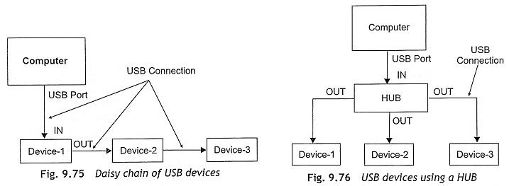
In the mid 1990’s, the Universal Serial Bus was invented by a group of companies such as IBM, Intel, Microsoft, Compaq, etc., and it was introduced as a high speed replacement of RS-232 serial port. It has very high bandwidth and operates at 1.5 MBps, 12 MBps and 480 MBps. This device can be used as daisy-chained as shown in Figure 9.75. The USB can also be used as multipoint bus and hubs provide multiple connection points for I/O devices as depicted in Figure 9.76. It can support about 127 devices. The commonly used USB devices are keyboard, monitors, digital cameras, mobile phones, digital video recorders, etc. The USB is available in different standards such as USB 1.1, USB 2.0 and USB on the go (OTG). This is low cost and hot plug-in play type. The hot plug-in play means the ability of USB to connect a device to the computer while a computer is in operation.
There are two basic requirements for USB implementation in microcomputers. The first is the presence of USB hubs to support USB ports on the microcomputer, and the second is the software support required from the operating system to operate the USB properly. Presently, all motherboards have built-in support for USB. The operating systems such as Window 98, Windows 95, OSR 2, Windows XP and other later versions can support USB. Whenever any device is connected into USB, the operating system would recognize the device and also configure the device simultaneously. The advantages of USB over the RS 232 are higher operating speed, ability to daisy chain connected different devices and support for hot plug and play.
Parallel Printer Interface
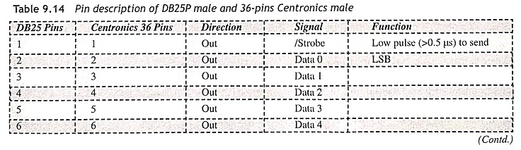
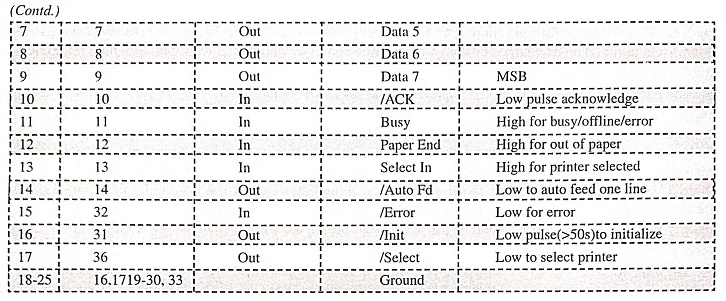
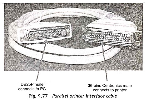
The parallel interface implies a Centronics-compatible printer interface. This interface was developed by the printer-manufacturing company Centronics and introduced on IBM PC in 1981 as line printer (LPT) port. The improved version of LPT was developed by Intel, Xircon and Xenith in 1994 and was known as Enhanced Parallel Port(EPP).The data-flow rate through a parallel interface is about 150 kbytes/s for LPT to 1.5 Mbytes/s for EPP. The typical parallel printer interface with a cable is shown in Figure 9.77. The pin description of DB 25 and Centronics are given in Table 9.14.
RS-232C
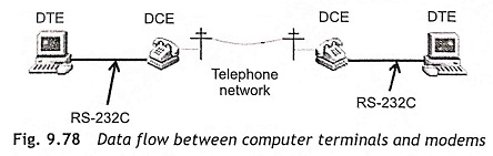
The serial communication is the simplest form of communication between two devices. Serial data transmission is used for digital communication between computers and computers, computers and peripheral devices (modems, printers, etc.) and sensors and computers for data acquisition. In all personal computers, serial interface is implemented using a communication port or COM port. There are four COM ports such as COM-1, COM-2, COM-3, and COM-4. The COM ports conform to the RS-232C interface standard. The RS-232C was developed by the Electronics Industry Association (EIA) in the 1960s. Actually, RS-232C was intended as an electrical specification to connect computer terminals to modems through DTE and DCE as shown in Figure 9.78. DTE means Data Terminal Equipment, and DCE stands for Data Communication Equipment. The modem is also a data set. In Figure 9.78, the data communication is the digital data exchange between a mainframe computer and a remote computer. These computers are linked by telephone lines and modems are used at each end for signal translation.
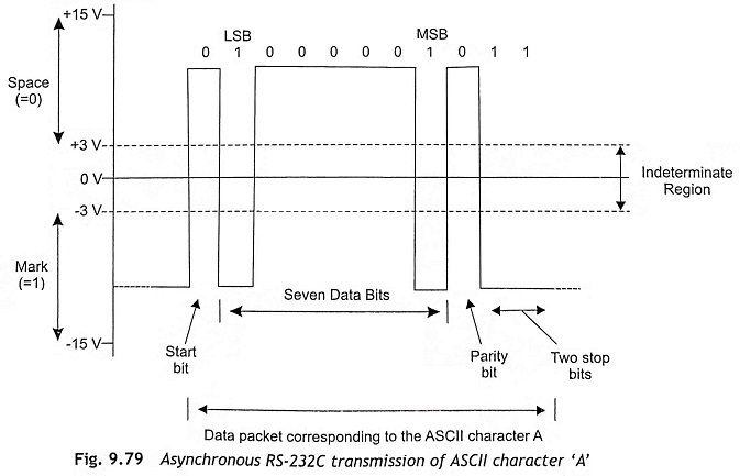
The maximum data flow rate of RS-232C is 20 kbits/s with a maximum cable length of 15 metres. The serial data transmission through RS-232C is possible in two different modes, namely, asynchronous and synchronous. In the asynchronous mode, the transmitting and receiving devices are not synchronized and the clock signal does not get transmitted along with the data. During synchronous mode, the transmitting and receiving devices are synchronized and the clock signal is transmitted along with the data. But most of the RS-232C operates in asynchronous mode. Data is transmitted on the Transmit Data (TD) line in packets (5 bits, 6 bits, 7 bits or 8 bits). Each packet consists of a start bit (0) at the beginning and a stop bit (1) at the end. A parity bit is also inserted at the end of the packet, but before the stop bit. The parity bit states either even parity or odd parity with the data bits in the packet.
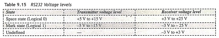
The line voltages of RS-232C have two states such as ON state and OFF state. The ON state is also known as marking state which is identified by a negative voltage. The OFF state is called the space state. The positive voltage is used to represent space state. In RS 232C, 1 is called a mark and 0 is called a space. The voltage limits of mark state and space state are given in Table 9.15. Figure 9.79 shows the plot of the asynchronous RS-232C transmission of ASCII character ‘A’ with start bit, parity bit and two stop bits.
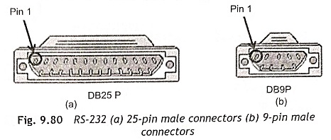
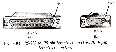
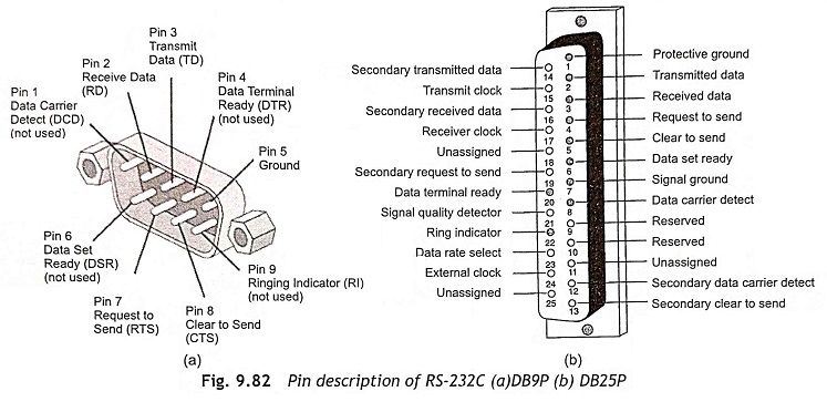
The original standard RS-232C is a 25-pin connector, but presently 9-pin RS-232C connectors are most commonly used. These connectors are available in male and female sockets. The DB25P and DB9P arc RS-232C 25 pin and 9-pin male connectors respectively as depicted in Figure 9.80. The DB25S and DB9S are RS-232C 25 pin and 9-pin female connectors respectively as illustrated in Figure 9.81. The detail description of RS-232C pins are given in Table 9.16 and Fig. 9.82. The function of signals as follows:
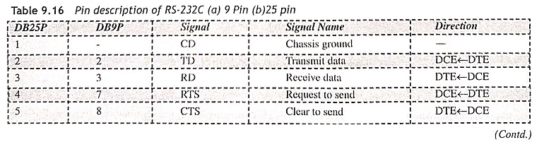
TD This signal is used to transmit data
RD This signal is used to receive data
DSR The DSR stands for data set ready. This signal indicates whether the DCE (modem) is powered ON.
DTR This is a data terminal ready signal which indicates whether DTR is powered on and turning off DTR causes modem to hang up the line.
RI The RI means Ring Indicator. This signal is activated by the modern when it detects incoming phone call on the telephone line.
DCD The Data Carrier Detect (DCD) is used by the modem to signal the transmitter that the communication link is usable. This signal is ON when two moderns have negotiated successfully and the carrier signal is established on the phone line.
RTS RST stands for Request To Send. This signal is activated when DTE wants to send data. This is used to turn on and off the modem’s carrier signal in multi-point lines, but usually it is constantly ON in point-to-point lines.
CTS The CRS stands for Clear To Send. This signal is used by the receiver to inform the transmitter that DCE is ready to receive data.
SG SG is Signal Ground.
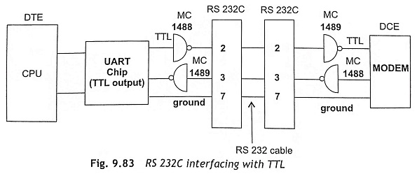
RS-232C with TTL Interfacing Figure 9.83 shows the interfacing RS 232C with TTL via special line drivers and receivers. The line driver MC 1488 can accept TTL level inputs and generates RS232C output levels. The MC 1488 converts logic level ‘1’ into about 9 V and logic level ‘0’ into +9 V. The MC 1489 converts RS-232C level inputs to TTL levels. The problem of RS-232C is that drivers and receivers are single ended. The input and output signals have a common ground.
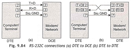
To interface a computer (CPU) and a peripheral device (modem), the minimum three lines such as 2, 3 and 7 are required as shown in Fig. 9.84. In the DTE to DCE communication, transmits on pin 2 and receives on pin 3 are as shown in Fig. 9.84(a). In DTE to DTE communication, the terminal transmits on Pin2 and receives on Pin 3 as shown in Fig. 9.84(b).
For high-speed data transmission, the standards RS-422A and RS-423A are used. Differential amplifiers are used in these standards to reduce noise levels and can transmit data at higher speed for long-distance cable. The RS 422A has a maximum speed of 10M baud for 40-feet distance and 10 kbaud for 1000-feet distance.
The speed of RS-423A is limited up to 100 kbaud for 130-feet distance and 10 kbaud for 300-feet distance.
IEEE-488 Bus
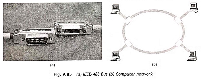
The General Purpose Interface Bus (GPIB) is known as Hewlett-Packard interface bus(HPIB) or IEEE488 bus. This was developed by Hewlett-Packard to interface testing equipment’s with a computer as shown in Fig. 9.85(a). These buses are used in a computer network as shown in Fig. 9.85(b). Usually, three types of standard devices such as listener, talker and controller can be connected on the GPIB.
The listener can receive data from other instruments or from the controller. For example, printers, display devices, programmable power supplies and programmable signal generators are used as listeners. A talker can send data to the instruments. The examples of talkers are tape readers, digital multimeters, frequency counters and measuring equipment’s. The third device, controller, determines who talks and who listens on the bus.
The IEEE-488 bus consists of a 24-wire cable with a connector such as that shown in Fig. 9.85(a). The IEEE-488 bus is an 8-bit parallel bus which allows up to 15 devices connected to the same computer port. This bus can be used as daisy-chain connectors and each cable is 2 in or less in length. Extensive handshaking controls the bus and many testing and measuring devices are equipped with GPIB. This bus can transfer data at reasonably fast speed of about 1 Mbit/s.
The IEEE-488 bus has five bus management lines such as IFC, ATN, SQR, REN and EOI. The IFC stands for interlace clear line. When this line is asserted by the controller, it resets all devices on the bus to a starting state. When the Attention Line (ATN) is active low, it indicates that the controller is putting a universal command or an address command on the data bus. If the ATN line is high, the data lines contain data or a status byte. The Service Request (SQR) can work as an interrupt. Whenever any device requires to transfer data on the data bus, the SQR line becomes low. After that the controller can pools all the devices to find the device which needs service. The Remote Enable Signal (REN) allows an instrument to be controlled directly h the controller. The End Of Identify (EOI) signal is used by a talker to indicate the completion of data transfer. This bus has three handshake lines such as Data Valid (DAV), Not Ready For Data (NRFD) and Not Data Accepted (NDAC). These lines are used to coordinate the transfer of data bytes on the data bus. The difference between RS-232C and IEEE-488 is given in Table 9.17.