Timing Diagram of the 8088 Microprocessor:
Each bus cycle of the 8088 processor consists of four T states: T1, T2, T3 and T4. During the first clock cycle T1, ALE signal is high and A19/S6-A16/S3 are used as A19-A16 address buses, AD7-AD0 can be used as A7-A0 address buses. Hence, the leading edge of ALE is used to latch the valid 20-bit address during T1 states. After T1 state A19/S6-A16/S3 are used as status signals S6-S3, the middle bus A15-A8 are always active as address buses but AD7-AD0 are tristated.During T3 and T4 data are read from memory and placed into the data bus. Therefore, AD7-AD0 is used as data bus in T3 and T4 durations. Figure 5.26 shows the timing diagram of the 8088 Microprocessor for memory read operation of 8088 microprocessor. After T4 the next bus cycle will be started.
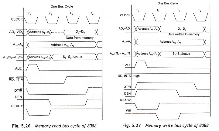
Figure 5.27 shows the timing diagram of the 8088 Microprocessor for memory write bus cycles. In memory cycle, data will be available on the data bus during T2, T3 and T4 and the status signals are valid for T2, T3 and T4 durations. After T4 address/data bus, AD7-AD0 arc tristated.