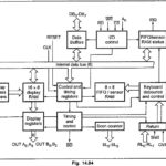
8279 Block Diagram
8279 Block Diagram: Fig. 14.84 shows the 8279 Block Diagram. It consists of four main sections CPU interface and control section Scan section 8279 Keyboard section Display section 1.CPU Interface…
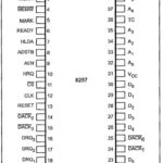
8257 Pin Diagram: Fig. 14.61 shows 8257 Pin Diagram. Data Bus (D0-D7) : These are bi-directional tri-state signals connected to the system data bus. When CPU is having control of…
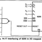
8255 Interfacing with 8086: Fig. 14.17 shows the 8255 Interfacing with 8086 Microprocessor and Interfacing 8255 with 8085 Microprocessor in I/O mapped I/O technique. Here RD and WR signals are…
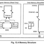
8051 Addressing Modes: The 8051 Addressing Modes architecture supports several distinct physical address spaces. On - chip program memory On - chip data memory External program memory External data memory…
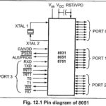
Intel 8051 Architecture and 8031 Architecture: Fig. 12.2 shows the Intel 8051 Architecture and 8031 Architecture. It consists of a Central Processing Unit, two kinds of memory (data RAM plus…
Features of 8051 Microcontroller: The Features of 8051 Microcontroller family are as follows. 1. Single-supply +5 volt operation using HMOS technology. 2. 4096 bytes program memory on-chip (not on 8031).…
Motorola 68000 Instruction Set: There are actually 56 basic instructions provided in the Motorola 68000 Instruction Set. With 14 addressing modes, 56 instructions, and 5 data types, the 68000 includes…
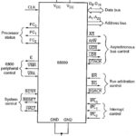
Motorola 68000 Pins and Signals: Fig. 11.3 illustrates the Motorola 68000 Pins and Signals. Data Transfer Control and Address Lines: D0-D15 is the bi-directional 16-bit data bus. A1-A23Â is the output…