Bridge Tied Load Amplifier:
All of the power amplifiers already discussed have been single-ended (SE): meaning that they provide power to a load that has one terminal grounded and the other terminal connected to the amplifier output. These amplifiers either use a plus-minus supply with directly-coupled loads, or have a capacitor-coupled load and a single-polarity supply. A Bridge Tied Load Amplifier (BTL) uses a single-polarity supply and a direct-coupled load.
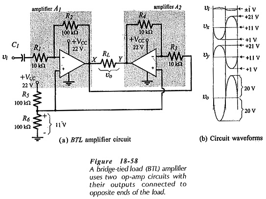
Figure 18-58(a) shows the basic circuit of a BTL amplifier. The two op-amps are connected to function as inverting amplifiers, but note from the resistor values that A1 has a voltage gain of 10 and that A2 has a gain of 1. Each amplifier has a single-polarity supply (VCC), and a voltage divider (R5 and R6) provides a bias voltage of 0.5 VCC to the op-amp noninverting input terminals. The load resistor (RL) is connected from the output of A1 to the output of A2. This is the Bridge Tied Load Amplifier configuration.
When no ac signal is applied, the dc voltage level at the load terminals (X and Y) is 0.5 VCC in this case, 11 V for a 22 V supply. As illustrated by the waveforms in Fig. 18-58(b), a +1 V ac input to A1 produces a -10 V change at load terminal X. This (-10 V) is also applied to the input of A2, resulting in a +10 V change at load terminal Y. Thus, a peak of 20 V is developed across the load, negative at X and positive at Y. When the ac input goes to -1 V, a 20 V peak load voltage is again produced, but with the load polarity reversed. So, although a single-polarity +22 V supply is used, the output is 40 V peak-to-peak, and no load coupling capacitor is required. A (similar performance) single-ended amplifier producing a 40 V peak-to-peak output would require either a ±22 V supply for a direct-coupled load, or a +44 V supply for a capacitor-coupled load.
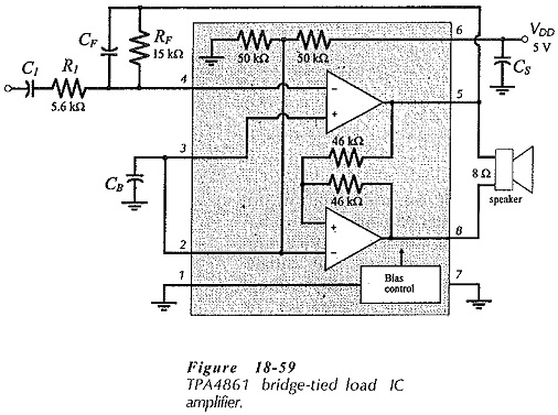
Figure 18-59 shows the pin connections and typical application of a TPA4861, 1 W integrated circuit BTL audio power amplifier. The load is connected across the two output terminals (5 and 8), external resistors R1 and RF set the voltage gain, and the signal is coupled to R1 via C1. The supply voltage (VDD) is internally divided to bias the op-amp noninverting terminals to 0.5 VDD. The bias point is externally accessible so that it can be bypassed to ground (via CB) for soft start-up and to minimize noise.
A TPA4861 using a +5 V supply can dissipate 1 W in an 8 Ω load. The overall voltage gain for the (BTL) amplifier is twice the gain of the inverting amplifier stage,
Because the signal is applied to an inverting amplifier, the input resistance is set by resistor R1. The IC manufacturer recommends that R1 should be selected in the range of 5 kΩ to 20 kΩ. Also, if RF exceeds 50 kΩ a small capacitor (CF = 5 pF) should be connected in parallel with it for ac stability.
The input capacitor (C1) sets the circuit low cutoff frequency. So,
![]()
The internal voltage divider resistance (50 kΩ||50 kΩ) is connected in series with the bypass capacitor (CB). The impedance of CB should typically be one tenth of the series resistance;
![]()
7 W IC Power Amplifier:
The LM383 can deliver 7 W to a 4 Ω load. No additional output transistors are required because the amplifier can produce a 3.5 A peak output current. Overload protection circuitry is included, and internal bias is provided for the input terminals. The single-polarity supply voltage ranges from 5 V to 20 V. Amplifier voltage gain can be programmed by means of external components. The circuit bandwidth is 30 kHz at a gain of 40 dB.
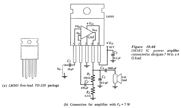
Figure 18-60 shows an LM383 (in a 5 pin TO220 package) connected to function as a (non-inverting) audio amplifier. Capacitors C1 and C4 are for coupling the signal and load. Resistors R1 and R2 are feedback components that set the circuit voltage gain, and capacitor C2 couples the feedback voltage to the inverting input terminal. Other components are for circuit stability. Note that the resistance of R2 is 2.2 Ω. This is because the inverting input terminal is connected to a transistor emitter terminal (internally) that has an input resistance around 20 Ω. Capacitor C2 must be very large to couple the feedback voltage to the (low resistance) inverting input. The circuit functions as a noninverting amplifier.
68 W IC Power Amplifier:
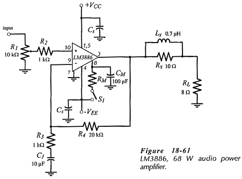
Figure 18-61(a) shows a power amplifier circuit using an LM3886 IC audio amplifier. The LM3886 can deliver 68 W to a 4 Ω load using a ±28 V supply. Alternatively, it can be used to dissipate 38 W in an 8 Ω load, again using a ±28 V supply. The circuit operates as a noninverting amplifier with the closed-loop gain set by resistors R3 and R4, and the low cutoff frequency set by capacitor C1. Potentiometer R1 allows the signal amplitude to be adjusted. Switch S1 is a mute control.