Op Amp Differential Amplifier Circuit Diagram and its Operation:
An ideal difference amplifier amplifies only the difference between two signals; it rejects any common signals to the two input terminals. For instance, a microphone system amplifies an audio signal applied to one terminal of a difference amplifier, and rejects any 50 Hz noise signal or “hum” existing on both terminals. The basic op-amp circuit also amplifies the difference between two input signals. However, we would like to make a difference amplifier, in which the output is a function of the ratio of resistors, as we had for the inverting and noninverting configurations. A circuit that amplifies the difference between two signals is called a difference or Op Amp Differential Amplifier. This type of amplifier is very useful in instrumentation circuits. A typical circuit is given in Fig. 34.29.
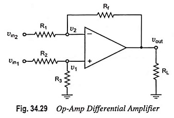
As already known, in a Op Amp differential amplifier, neither input is grounded. This reduces the amount of noise injected into the amplifier, because any noise appears simultaneously on both input terminals and the amplifying circuitry rejects it being a common mode signal.
A close examination of the circuit given in Fig. 34.29 reveals that it is a combination of inverting and noninverting amplifiers. When vin1 is zero, the circuit appears as an inverting amplifier while when vin2 is zero the circuit becomes a noninverting amplifier.
Since the circuit has two inputs vin1 and vin2, superposition theorem will be used for determination of voltage gain of the amplifier.
When vin1 is zero volt, circuit becomes an inverting amplifier and, therefore, output voltage due to vin2 is
Now assuming vin2 = 0, the circuit is a noninverting amplifier having a voltage-divider network consisting of resistor R2 and R3 at the noninverting input. Therefore,
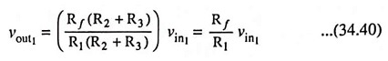
and output due to vin1 then is
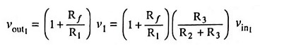
If R1 = R2 and Rf = R3
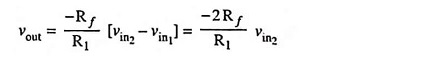
The net output voltage,
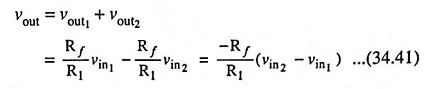
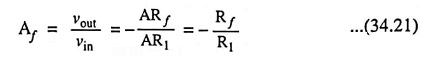
Differential voltage gain,
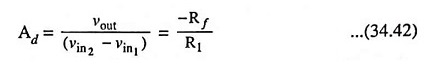
The above equation resembles Eq. (34.21) and hence the gain of the differential amplifier is same as that of inverting amplifier.
Such a circuit is very useful in detecting very small differences in signals, since the gain Rf/R1 can be selected to be very large. For instance if Rf = 500 R1, then a small difference of vin2 – vin1 is amplified 500 times.
The Op Amp differential amplifier can be operated in three different modes:
1. Single Ended Mode: The Op Amp differential amplifier is in a single ended mode when input signal is applied to only one of the two input terminals i.e., either of the two inputs is zero. Thus in this mode, the differential amplifier will act either as an inverting amplifier or as a noninverting amplifier depending on whether the signal is applied to the inverting or noninverting terminal.
2. Differential Mode: In this mode of operation, magnitude of the two input signals may be same or different but their polarity is opposite at every instant of time i.e.,
![]()
So input voltage,
![]()
Hence
3. Common Mode: In this mode the two input signals are same in magnitude as well as in phase at every instant of time
So input voltage,
![]()
and output voltage is zero.
Thus there is no output voltage when the differential amplifier is connected in common mode.
Input Resistance:
The input resistance, Rin of the Op Amp differential amplifier is the resistance worked out looking into either one of the two input terminals with the other grounded.
Hence with vin1 = 0 V, the circuit given in Fig. 34.29 becomes that of an inverting amplifier, the input resistance of which is
![]()
Similarly with vin2 = 0 V, the circuit given in Fig. 34.29 becomes that of noninverting amplifier whose input resistance is given as
![]()
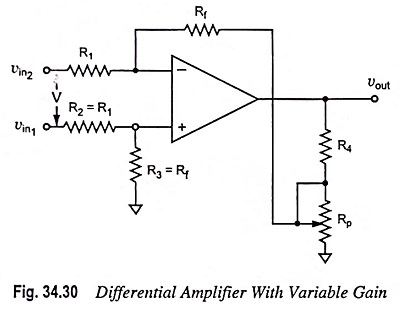
Equations (34.43) and (34.44) reveal that the input resistance looked into by the signal sources vin1 and vin2 is not the same. For proper functioning of amplifier circuit given in Fig. 34.29, it is necessary that resistances R1 and (R2 + R3) are made much larger than source resistances so as to avoid loading of signal sources. In cases where a variable gain is required, the circuit given in Fig. 34.29 is modified by introducing a potentiometer as depicted in Fig. 34.30. The voltage gain can be varied from the closed-loop gain of -2Rf/R1 to the open-loop gain of A.