Op Amp IC 741 Pin Diagram and its Working:
The schematic diagram and Op Amp IC 741 Pin Diagram is shown in Fig. 33.4 (a) and in Fig. 33.4 (b). It is not necessary to understand every detail about the circuit design and its operation in order to be able to use the IC. What must be understood is the correct terminal connection and biasing for the input terminal, as well as the limitations on supply voltages, signal levels, and external load. In the schematic diagram shown in Fig. 33.4 (a), the base leads of Q1 and Q2 are connected to the pins on the IC unit and serve as the two inputs of the op-amp. Q1 and Q2 transistors form a differential amplifier circuit. Transistors Q12 and Q13 constitute a complementary emitter follower output stage. The output is taken at the emitter of transistors Q12 and Q13. This push-pull configuration allows the op-amp to have a very low output impedance, which is analogous to a voltage source having a very small internal resistance.
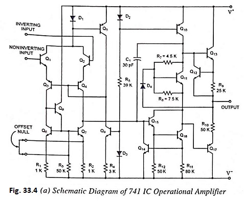
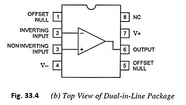
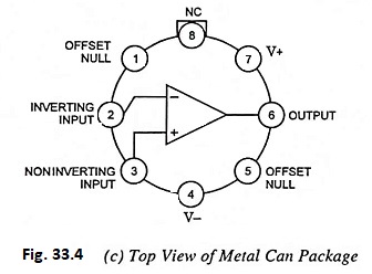
Figure 33.4 (b) shows the IC 741 Pin Diagram connection terminals for a single Op Amp IC 741 in a dual-in-line package, and Fig. 33.4 (c) shows the connection terminals for a Op Amp IC 741 enclosed in a metal can package. From Figs. 33.4 (b) and 33.4 (c) it is obvious that there are two input terminals (pins 2 and 3) and one output terminal (pin 6). Both a positive (pin 7) and negative (pin 4) supply voltage must be furnished.
Op Amp IC 741 Pin Diagram:
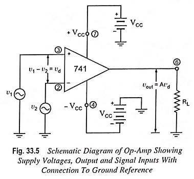
The schematic arrangement showing the output and input signals and the positive and negative power supplies is shown in Fig. 33.5. The op-amp can accommodate a positive as well as a negative input signal simultaneously or either one separately. The signal v1 is applied to pin 3, which produces a noninverting output i.e., output voltage appearing at pin 6 has the same polarity as the input signal voltage. The signal v2 is applied to pin 2, which produces an inverting output (the internal circuitry of the op-amp yields an output signal of inverted or opposite polarity). The design of the op-amp is such that the output voltage is related to the two input voltages by equation
![]()
Keep in mind that v1 denotes the voltage that is applied to the noninverting terminal (pin 3) and v2 is the signal applied to the inverting terminal (pin 2) and vd is the net differential input voltage. The quantity A is the open-loop gain of the op-amp and customary has values of 100,000. This means that the net differential input voltage is raised at the output terminal (pin 6) by this factor. Clearly, then, if overloads are to be avoided, it is essential to limit vd to those values that will keep output voltage vout at least below the magnitude of the supply voltage VCC. Accordingly, for the case where A = 1 x 10⁵ it follows that vd must be limited to
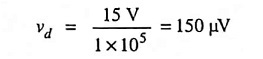
which is obviously a very small quantity. Fortunately, there are techniques for increasing this limit to more practical values.
To make the amplifier free from common-mode undesired signals, like from pickups etc., neither of its input terminals should be grounded. This can be achieved by using differential input mechanism in which both the input terminals are at same voltage level with respect to ground. One terminal is noninverting terminal and the other is inverting terminal.