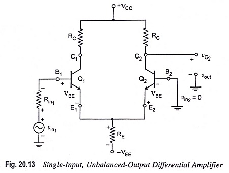
Single Input Unbalanced Output Differential Amplifier
Single Input Unbalanced Output Differential Amplifier: Single input unbalanced output differential amplifier configurations are rarely used. The reasons for this are as follows: This configuration is identical to the CE amplifier but it needs comparatively…
Comments Off on Single Input Unbalanced Output Differential Amplifier
November 26, 2022