Voltage Follower Circuit Diagram:
Direct-Coupled Voltage Follower – The IC operational amplifier can be employed for an infinite variety of applications. The very simplest application is the direct-coupled Voltage Follower Circuit Diagram shown in Fig: 14-10(a). The output terminal is connected directly to the inverting input terminal, the signal is applied to the noninverting input, and the load is directly-coupled to the output.
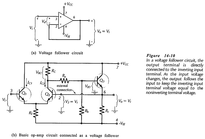
Figure 14-10(b) shows the basic op-amp circuit connected as a Voltage Follower Circuit Diagram. With the differential amplifier input stage, V2 (which equals Vo) must equal Vi. When V2 is higher or lower than Vi, the voltage difference is amplified to move the output back to equality with the input.
Suppose Vo was slightly higher than Vi. The voltage at Q2 base (terminal 2) would be higher than that at Q1 base (terminal 3), therefore IC2 would be increased above its normal level. This would cause an increase in the voltage drop across RC, thus reducing VB3 and driving Vo back to equality with Vi. Similarly, when Vo is lower than Vi, Q2 base voltage is lower than that at Q1 base, IC2 is reduced, thus reducing VRC, increasing VB3, and driving Vo back up toward Vi.
When the input voltage (at terminal 3) is increased or decreased, the feedback effect causes the output to almost perfectly follow the input. The actual difference between the input and output voltage is easily calculated from the output voltage level and the op-amp open-loop voltage gain.
Like an emitter follower, the Voltage Follower Circuit Diagram has a high input impedance a low output impedance, and a voltage gain of 1. The Voltage Follower Circuit Diagram performance is superior to that of the emitter follower.
Capacitor-Coupled Voltage Follower:
When a voltage follower is to have capacitor-coupled input and output terminals, the noninverting input must be grounded via a resistor, [see (R1) Fig. 14-12]. As discussed, the resistor is required for passing bias current to the noninverting input terminal. It also offers an input resistance to the signal source, rather than a short-circuit. Because the load is capacitor-coupled, the dc output offset voltage might seem to be unimportant. However, the dc offset voltage at the op-amp output terminal can limit the amplitude of the output voltage. So, a resistor (R2) equal to R1 should be included in series with the inverting input terminal to equalize the IBRB voltage drops and thus minimize output offset voltage, as already discussed.
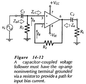
Design of the capacitor-coupled circuit in Fig. 14-12 involves calculation of R1, C1, and C2. The circuit input impedance is R1||Zi, however, Zi is always much larger than R1. So, the circuit input impedance is simply taken as,
![]()
Normally, The load resistance RL is much smaller R1, and consequently, the smallest capacitor values are calculated when C2 is selected to set f1. Therefore,
![]()
Capacitor C1 should then be calculated from, XC1 = (Zin + rs)/10 at f1, so that it has no significant effect on the circuit lower cutoff frequency.
![]()