Photodiode Operation and Characteristics:
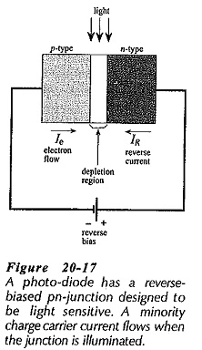
Photodiode Operation – When a pn-Junction is reverse biased, a small reverse saturation current flows due to thermally generated holes and electrons being swept across the junction as minority charge carriers. Increasing the junction temperature generates more hole-electron pairs, and so the minority carrier (reverse) current is increased. The same effect occurs if the junction is illuminated, (see Fig. 20-17). Hole-electron pairs are generated by the incident light energy, and minority charge carriers are swept across the junction to produce a reverse current flow. Increasing the junction illumination increases the number of charge carriers generated, and thus increases the level of reverse current. Diodes designed to be sensitive to illumination are known as photodiodes.
Characteristics:
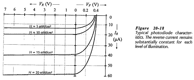
Consider the typical photodiode illumination characteristics in Fig. 20-18. When the Junction is dark, the dark current (ID) would seem to be zero. Typically, ID is around 2 nA. A 20 mW/cm2 illumination level produces a reverse current of approximately 60 μA. Increasing the reverse voltage does not increase IR significantly. So, each characteristic is approximately a horizontal line.
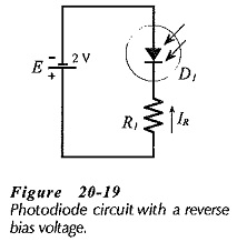
Figure 20-19 shows a simple photodiode circuit using a 2 V reverse bias. (Note the device circuit symbol.) Assuming that D1 has the characteristics in Fig. 20-18, the current at a 5 mW/cm2 illumination level is approximately 13 μA. At 20 mW/cm2 the diode current is around 60 μA. The device resistance at each illumination level is readily calculated: (at a 5 mW/cm2, R = 2 V/ 13 μA = 154 kΩ), (at a 20 mW/cm2, R = 2 V/60 μA = 33 kΩ). The resistance changed by a factor of approximately 5 from the low to the high illumination level, showing that a Photodiode Operation can be employed as a photoconductive device.
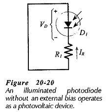
When the reverse-bias voltage across a photodiode is removed, minority charge carriers continue to be swept across the junction while the diode is illuminated. With an external circuit connected across the diode terminals, the minority carriers flow back to their original sides. The electrons that crossed the junction from p to n will now flow out through the rt-terminal and into the p-terminal. This means that the device is behaving as a voltage cell, with the n-side being the negative terminal and the p-side the positive terminal, as illustrated in Fig. 20-20. In fact, a voltage can be measured at the photodiode terminal, positive on the p-side and negative on the n-side. So, the photodiode is a photovoltaic device as well as a photoconductive device. The characteristics in Figure 20-18 show that, when illuminated, the photodiode actually has to be forward biased to reduce the reverse current to zero.
It should be noted that VR and VF have different scales on the photodiode characteristics shown in Fig. 20-18. A dc load line that crosses between the forward and reverse biased regions cannot be drawn on these characteristics. Equal scales must be used for each part of the characteristics to draw such a load line.
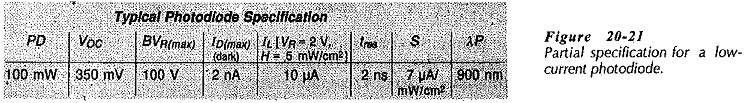
Specification:
A partial specification for a typical Photodiode Operation is shown in Fig. 20-21. The light current (IL) is listed as 10 μA at an illumination level of 5 mW/cm2 when the reverse bias is 2 V. This is sometimes defined as a short-circuit current (ISC). The dark current (ID) is specified as 2 nA maximum when the reverse voltage is 20 V, and the open-circuit terminal voltage (VOC) is given as 350 mV. Note that the typical response time (tres) of 2 ns for a photodiode is very much superior to that for a photoconductive cell. The diode sensitivity (S) is the change in diode current produced by a given change in light intensity. The power dissipation, reverse breakdown voltage, and peak output wavelength are also listed.
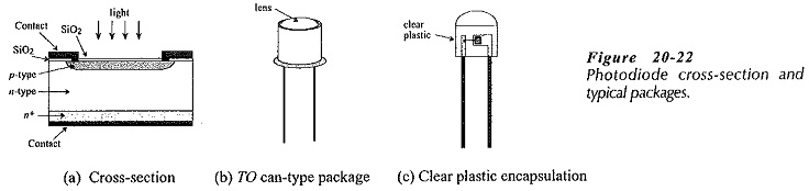
Construction:
Figure 20-22(a) shows the cross-section of a diffused photo diode. It is seen that a thin heavily-doped p-type layer is situated at the top where it is exposed to incident light. The junction depletion region penetrates deeply into the lightly-doped n-type layer. This is in contact with a lower heavily-doped n-type layer which connects to a metal film contact. A ring-shaped contact is provided at the top of the p-type layer. Low-current photodiodes (also called signal photodiodes) are usually contained in a TO-type can with a lens at the top, [see Fig. 20-22(b)]. Clear plastic encapsulation is also used, [Fig. 20-22(c)].
Photodiode Applications:
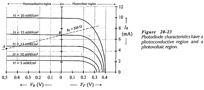
Photodiodes can be used as photoconductive devices in the type of circuits. They can also be used in circuits where they function as photovoltaic devices. Figure 20-23 shows typical photodiode characteristics plotted in the first and second quadrants for convenience. When the device is operated with a reverse voltage, it functions as a photoconductive device. When operating without the reverse voltage, it operates as a photovoltaic device. In some circuits the photodiode can change between the photoconductive mode and the photovoltaic mode.