Oscillator Amplitude Stabilization Circuit:
Output Amplitude – For all of the Oscillator Amplitude Stabilization Circuit discussed, the output voltage amplitude is determined by the amplifier maximum output swing. The output waveform may also be distorted by the amplifier output saturation limitations. To minimize distortion and reduce the output voltage to an acceptable level, amplitude stabilization circuitry must be employed. Oscillator Amplitude Stabilization Circuit operates by ensuring that oscillation is not sustained if the output exceeds a predetermined level.
Diode Stabilization Circuit for a Phase Shift Oscillator:
The phase shift oscillator discussed earlier must have a minimum amplifier gain of 29 for the circuit to oscillate. Consider the oscillator circuit in Fig. 16-12(a) that has part of resistor R2 bypassed by series-parallel connected diodes. When the output amplitude is low, the diodes do not become forward biased and so they have no effect on the circuit. At this time, the amplifier voltage gain is, ACL = R2/R1. As always for a phase shift oscillator, ACL is designed to exceed the critical value of 29. When the output amplitude becomes large enough to forward bias either D1 and D2, or D3 and D4, resistor R4 is short-circuited, and the amplifier gain becomes, ACL = R5/R1. This is designed to be too small to sustain oscillations. So, this circuit cannot oscillate with a high-amplitude output, however it can (and does) oscillate with a low-amplitude output.
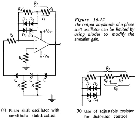 In designing the Oscillator Amplitude Stabilization Circuit, the inverting amplifier is designed in the usual manner with one important difference. The current (I1) used in calculating the resistor values must be selected large enough to forward bias the diodes into the near-linear region of their characteristics. This usually requires a minimum current around 1 mA. Resistor R1 is calculated using,
and R2 is determined as,
![]()
The diodes should become forward biased just when the output voltage is at the desired maximum level. At this time, I1 produces a voltage drop of 2 VF across R4,
and![]()
The resultant component values should give (R4 + R5)/R1 slightly greater than 29, and R5/R1 less than 29.
Some distortion of the waveform can occur if (R4 + R5)/R1 is much larger than 29, however, attempts to make the gain close to 29 can cause the circuit to stop oscillating. Making a portion of R5 adjustable, as illustrated in Fig. 16-12(b), provides for gain adjustment to give the best possible output waveform. Typically, R6 should be approximately 40% of the calculated value of R5, and R7 should be 80% of R5. This gives a ±20% adjustment of R5.
The diodes selected should be low-current switching devices. The diode reverse breakdown voltage should exceed the circuit supply voltage, and the maximum reverse recovery time (trr(max)) should be around one-tenth of the time period of the oscillation frequency,
Diode Stabilization Circuit for a Wein Bridge Oscillator:
Figures 16-14, and 16-15 show two output, Oscillator Amplitude Stabilization Circuit methods that can be used with a Wein bridge oscillator. These can also be applied to other oscillator circuits, because they all operate by limiting the amplifier voltage gain
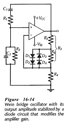
The circuit in Fig. 16-14 uses diodes and operates in the same way as the amplitude control for the phase-shift oscillator. Resistor R6 becomes shorted by the diodes when the output amplitude exceeds the design level, thus rendering the amplifier gain too low to sustain oscillations.
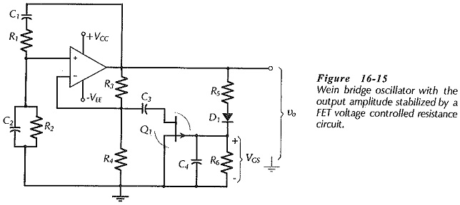
FET Stabilization Circuit for a Wein Bridge Oscillator:
The circuit in Fig. 16-15 is slightly more complex than the diode circuit, however, like other circuits, it stabilizes the oscillator output amplitude by controlling the amplifier gain. The channel resistance (rDS) of the p-channel FET (Q1) is in parallel with resistor R4. Capacitor C3 ensures that Q1 has no effect on the amplifier dc conditions. The amplifier voltage gain is,
The FET gate-source bias voltage is derived from the amplifier ac output. The output voltage is divided across resistors R5 and R6, and rectified by diode D1. Capacitor C4 smoothes the rectified waveform to give the FET dc bias voltage (VGS) . The polarity shown on the circuit diagram reverse biases the gate-source of the p-channel device. When the output amplitude is low, VGS is low and this keeps the FET drain-source resistance (rDS) low. When the output gets larger, VGS is increased causing rDS to increase. The increase in rDS reduces ACL, thus preventing the circuit from oscillating with a high output voltage level. It is seen that the FET is behaving as a voltage variable resistance (VVR).
Design of a FET Stabilization Circuit:
To design the FET Oscillator Amplitude Stabilization Circuit, knowledge of a possibly suitable FET is required; in particular, the channel resistance at various gate-source voltages must be known.
Suppose the circuit is to oscillate when rDS = 6 kΩ at VGS = 1 V, and that the peak output is to be Vo(pk) = 6 V. Resistors R5 and R6 should be selected to give VGS = 1 V when Vo(pk) = 6 V, allowing for VF across the diode. Capacitor C4 smoothes the half-wave rectified waveform, and discharges via R6 during the time interval between peaks of the output waveform. The capacitance of C4 is calculated to allow perhaps a 10% discharge during the time period of the oscillating frequency. The voltage divider current (I5) should be a minimum of around 100 μA for satisfactory diode operation.
C3 is a coupling capacitor; its impedance at the oscillating frequency should be much smaller than the rDS of the FET. Resistors R3 and R4 are calculated using Eq. 16-19 to give the required amplifier voltage gain when rDS = 6 kΩ.