Binary Ladder Circuits:
A Binary Ladder Circuits is constructed of resistors having only two values and thus overcomes the disadvantages of weighted resistors. The left end of the ladder is terminated in 2 R, as shown in Fig. 17.14.
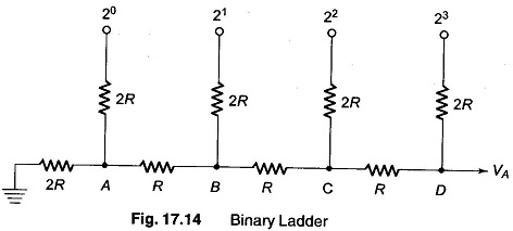
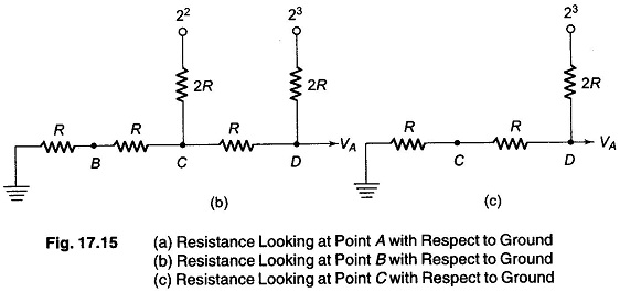
Assuming that all digital inputs are at ground, beginning at point A of Fig. 17.14, the total resistance looking into the terminating resistors is 2R, as seen from Fig. 17.15(a). The total resistance looking out towards the 20 input is 2R. These two resistors combine to form a value of R. At node B or at 21, the input is still 2R, as seen from Fig. 17.15(b). It is clear from Fig. 17.15(c) that the resistance looking back towards node C is 2R, as is the resistance looking at the 23 input.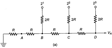
From this we conclude that the resistance looking back from any node towards the terminating resistance or out toward the digital input is 2R. We can use this to determine the various digital inputs. First, assume that the digital input signal is 1000, as shown in Fig. 17.16.
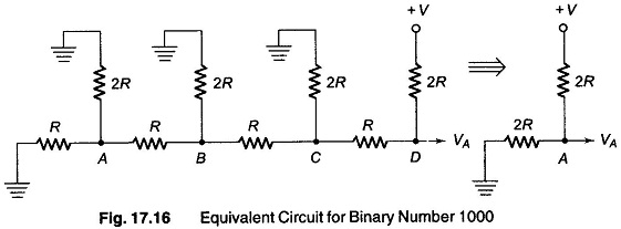
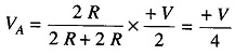
Since there is no voltage source to the left of the node D, it can be replaced by 2R.
therefore
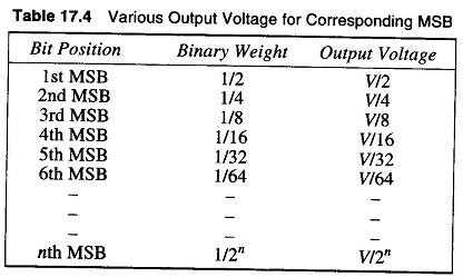
Hence a 1 in the MSB position provides an output voltage of +V/2.
To determine the output voltage due to the 2nd MSB, assume an input of 0100, as shown in Fig. 17.17(a).
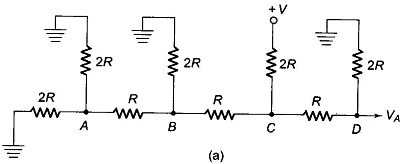
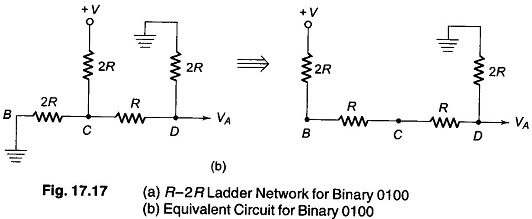
Therefore, the left side network of node C with its The’venin equivalent, is clearly a resistance R in series with a voltage source of +V/2. The final equivalent circuit, the The’venin’s equivalent include, is
Hence the 2nd MSB equals + V/4. This process can be continued, and it can be shown that the 3rd MSB gives an output voltage of + V/8, the 4th MSB gives an output voltage of +V/16 and so on.
The various output voltages for the corresponding MSB are given in Table 17.4.