Sampling Circuits:
Sampling Circuits is one which allows a comparison of instantaneous values derived at different instants of time, thereby dispensing with the need to phase shift and mix signals derived from the primary line quantities.
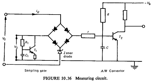
Figure (10.36) shows a sampling circuits in conjunction with an amplitude pulse width convertor (A/W convertor), this complete circuit forms the measuring unit for a relay. The circuit works as follows.
When iG is zero, a very high impedance is inserted between the signal voltage VS and A/W convertor. The maximum VS must be less than the breakdown voltage of the zener diode, otherwise conduction can take place via the zener diode and the VG source impedance. When iG is nonzero, i.e. during the 50μs sampling period provided that iS<iG the resistance of the bridge between VS and the A/W convertor is small.
The current iG is caused by the application of a rectangular 50μs voltage pulse VG to the diode bridge, where VG is large enough to break through the zener diode. It is found that the stray capacitance of the bridge diodes and the zener diode are such as to allow a very fast positive going edge to produce a spike at the output, even though iG is zero. The circuit comprising
T1,R1 and C1 is added to deal with this contingency. The time constant R1 C1 is such that T1 is held off except when VS attempts to increase rapidly. Purely by considerations of cause and effect this circuit cannot remove a spike from VS, but by switching on T1 and drawing a spike of current through the signal source impedance, the rate of rise of discontinuity is slowed down sufficiently to prevent it getting through the diode bridge.
During the 50μs sampling period, C charges up through the resistance r+RS, where RS is the signal source resistance. R>r+RS and can therefore be neglected during the charging period. At the end of the sampling period, C commences to discharge through R towards the negative supply voltage. The diode bridge resistance is now very much larger than R and can be neglected during the discharge period.
The transistor T2 is normally on and is switched off at the start of the sampling period as the voltage on C goes positive. It switches on again when the voltage on C is approximately zero. The output at the collector of T2 is therefore a pulse of length T’ which is proportional to VS at the instant of Sampling Circuits provided that T′≪CR.