Variable Resistor Network:
Variable Resistor Network – The basic problem in converting a digital signal into an equivalent analog signal is to change the n digital voltage levels into one equivalent analog voltage. This can be achieved most easily by designing a Variable Resistor Network which changes each of the digital levels into an equivalent binary weight voltage (or current). To understand the meaning of equivalent binary weight consider the truth table for the 3 bit binary signal shown in Table 17.1.
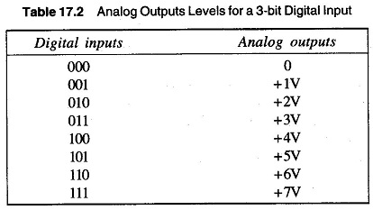
Suppose we wish to change the 8 possible states of digital signals into equivalent analog voltages. The smallest number represented by 000 is OV and the largest number represented is 111. Let us make this signal equal to + 7V. This then establishes the range of the analog signal which will be developed. Now, between 000 and 111 there are seven discrete levels to be defined. Therefore, it is convenient to divide the analog signal into seven levels.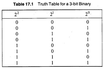
The smallest increment change in the digital signal is represented by the LSB (20). Hence we would like to have this bit cause a change in the analog output equal to 1/7 of the full scale analog output voltage. The resistive divider will then be designed such that a 1 in the 20 position causes + 7 x 1/7 = 1 V at the output.
Since 21 = 2 and 20 = 1, it can be seen that the 21 number is twice the size of the 20 bit. Therefore a 1 in the 21 bit position must cause a change in the analog output voltage which is twice the size of the LSB. The resistive divider must then be designed such that a 1 in the 21 bit position causes a change of + 7 x 2/7 = + 2 V in the analog voltage.
Similarly, 22 = 4 = 21 x 2 = 4 x 20 this 22 bit must cause a change in the output voltage which is 4 times that of the LSB. The 22 bit must then cause an output voltage change of + 7 x 4/7 = + 4 V.
The process can be continued and it will be seen that each successive bit must have a value which is twice that of the preceding bit. Thus the LSB is given a binary equivalent weight of 1/7, or 1 part in 7. The next LSB is given a weight of 2/7, which is twice the LSB or 2 parts in 7. The MSB (in the case of a 3 bit system) is given by 4/7, which is 4 times the LSB or 4 parts in 7.
The total sum of the weights must be equal to 1. Hence
![]()
In general, the binary equivalent weights assigned to the LSB is 1/2n – 1 where n is the number of bits.
A resistive divider having three digital inputs and an analog output is shown in Fig. 17.9.
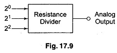
In this Variable Resistor Network case, assume digital levels 0 = 0 V and 1 = + 7 V.
For an input of 001, the output is + 1 V; similarly for 010, the output is + 2 V and for 100, the output is + 4 V. Now digital input of 011 is seen to be a combination of signals 001 and 010. If + 1 V from the 20 bit is added to + 2 V from the 21 bit, the output is + 3 V for an input of 011. Similarly, other levels are determined by an additive combination of voltages, as shown in Table 17.2.
Hence the resistive ladder must do two things in order to change the digital input into an equivalent analog output.
- 20 bit must be changed to +1 V, 21 bit to +2 V and 22 bit to + 4 V.
- The three voltages representing the digital bits must be summed together to form the analog output voltage.
A resistive ladder which performs the above functions is shown in Fig. 17.10.
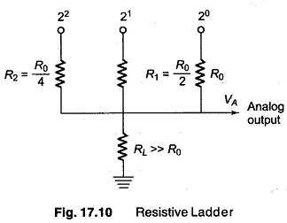
The resistors R0 , R1 and R2 form the divider network. RL is the load to which the divider is connected and is large enough not to load the divider network.
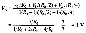
Assume that the digital input signal 001 is applied to this Variable Resistor Network. Using the levels as before, 0 = 0 V and 1 = +7 V. The equivalent circuit is shown in Fig. 17.11. RL. is considered very large, and hence neglected.
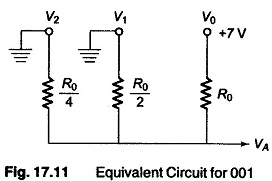
The analog output voltage VA can be easily determined by the use of Millman’s theorem.
Millman’s theorem states that the voltage appearing at any node in a resistive network is equal to the summation of the current entering the node (found by assuming the node voltage is 0) divided by the summation of the conductances connected to the node.
In equation form, Millman’s theorem states
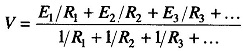
Applying Millman’s theorem to Fig. 17.11
In general, the following hold.
- There is one input resistance for each digital bit.
- Beginning with the LSB, each following resistor is half the previous
- The full scale output voltage is equal to the +ve voltage of the digital input signal (negative voltages work equally well).
- The change in output voltage due to a change in the LSB is equal to V/(2n — 1), where V is the digital input voltage level.
- The LSB has a weight of 1/(2n— 1), where n is the number of input bits.
- The output voltage VA can be found for any digital input signal by using the following modified form of Millman’s theorem.
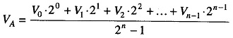
where V0, V1, V2, …, Vn-1 are the digital input voltage levels (0 and + V) and n is the number of input bits.
The Variable Resistor Network has two basic drawbacks.
- Each resistance in the network has a different value. Since the dividers are usually constructed using precision resistors, their cost factor increases.
- The resistance used in the MSB is required to handle a much larger current than the LSB resistor. (For example, the current through the MSB may be 500 times larger than that through the LSB.)
For these reasons, a second type of Variable Resistor Network, called a ladder is used.