Common Base Transistor Characteristics:
To investigate the Common Base Transistor Characteristics of a diode (a two-terminal device), several levels of forward or reverse bias voltage are applied and the resulting current levels are measured. The characteristics of the device are then derived by plotting the graph of current versus voltage. Because a transistor is a three-terminal device, there are three possible connection arrangements (configurations) for investigating its Common Base Transistor Characteristics. From each of these configurations, three sets of Common Base Transistor Characteristics may be derived.
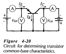
Figure 4-20 shows a pnp transistor with its base terminal common to both the input (EB) voltage and the output (CB) voltage. The transistor is said to be connected in common base configuration. Voltmeters and ammeters are included to measure the input and output voltages and currents.
Input Characteristics of Common Base Configuration:
To determine the Input Characteristics of Common Base Configuration, the output (CB) voltage is maintained constant, and the input (EB) voltage is set at several convenient levels. For each level of input voltage, the input current IE is recorded. IE is then plotted versus VEB to give the Input Characteristics of Common Base Configuration shown in Fig. 4-21.
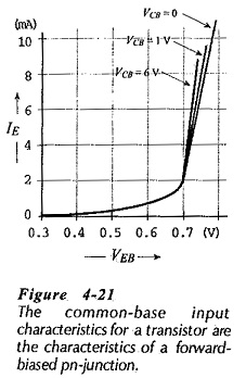
Because the EB junction is forward biased, the common-base input characteristics are essentially those of a forward biased pn-junction. Figure 4-21 also shows that for a given level of input voltage, more input current flows when higher levels of CB voltage are used. This is because larger CB (reverse bias) voltages cause the depletion region at the CB junction to penetrate deeper into the base of the transistor, thus shortening the distance and reducing the resistance between the EB and CB depletion regions.
Output Characteristics of Common Base Configuration:
The emitter current IE is held constant at each of several fixed levels. For each fixed level of IE, the output voltage VCB is adjusted in convenient steps, and the corresponding levels of collector current IC are recorded. In this way, a table of values is obtained from which a family of output characteristics may be plotted. In Fig. 4-22 the corresponding IC and VCB levels obtained when IE was held constant at 1 mA are plotted, and the resultant Common Base Transistor Characteristics is identified as IE = 1 mA. Similarly, other characteristics are plotted for IE levels of 2 mA, 3 mA, 4 mA, and 5 mA.
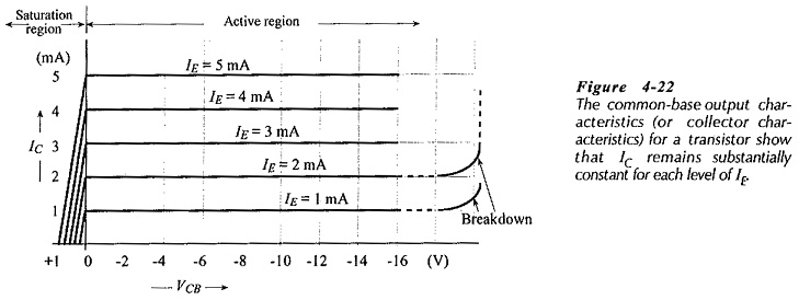
The Output Characteristics of Common Base Configuration is shown in Fig. 4-22 show that for each fixed level of IE, IC is almost equal to IE and appears to remain constant when VCB is increased. In fact, there is a very small increase in IC with increasing VCB. This is because the increase in collector-to-base bias voltage (VCB) expands the CB depletion region, and thus shortens the distance between the two depletion regions. With IE held constant, the increase in IC is so small that it is noticeable only for large variations in VCB.
As illustrated in Fig. 4-22, when VCB is reduced to zero, IC still flows. Even when the externally applied bias voltage is zero, there is still a barrier voltage existing at the CB junction, and this assists the flow of IC. The charge carriers which constitute IC are minority carriers as they cross the CB junction. Thus, the reverse-bias voltage VCB and the (unbiased) CB barrier voltage assist their movement across the junction. To stop the flow of charge carriers, the CB junction has to be forward biased.
Consequently, as shown in Fig. 4-22, IC is reduced to zero only when VCB is increased positively.
The region of the graph for the forward-biased CB junction is known as the saturation region, (see Fig. 4-22). The region in which the junction is reverse biased is named the active region, and this is the normal operating region for the transistor.
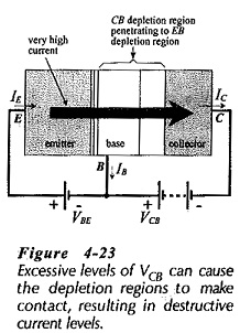
If the reverse-bias voltage on the CB junction is allowed to exceed the maximum safe limit specified by the manufacturer, device breakdown may occur. Breakdown, illustrated by the dashed lines in Fig. 4-22, can be caused by the same effects that make diodes breakdown. Breakdown can also result from the CB depletion region penetrating into the base until it makes contact with the EB depletion region, (Fig. 4-23). This condition is known as punch-through, or reach-through, and very large currents can flow when it occurs, possibly destroying the device. The extension of the depletion region is produced by the increase in VCB. So, it is very important to maintain VCB below the maximum safe limit specified by the device manufacturer. Typical maximum VCB levels range from 25 V to 80 V.
Current Gain in Common Base Configuration:
The current gain characteristics (also termed the forward transfer characteristics) are a graph of output current (IC) versus input current (IE). They are obtained experimentally by use of the circuit in Fig. 4-20. VCB is held constant at a convenient level, and IC is measured for various levels of IE. IC is then plotted versus IE, and the resultant graph is identified by the VCB level, (see Fig. 4-24).
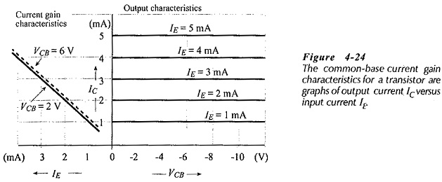
The CB current gain characteristics can be derived from the CB output characteristics, as shown in Fig. 4-25. A vertical line is drawn through a selected VCB value, and corresponding levels of IE and IC are read along the line. The IC levels are then plotted versus IE, and the characteristic is labelled with the VCB used. Because almost all of IE flows out of the collector terminal as IC, VCB has only a small effect on the current gain characteristics.