Summing Amplifier Circuit Diagram:
Figure 14.17 shows an Summing Amplifier circuit diagram in inverting configuration with three inputs Va, Vb, Vc. Depending on the relation between Ra, Rb, Rc and RF, the circuit can be used as a Summing amplifier, Scaling amplifier or Average amplifier.
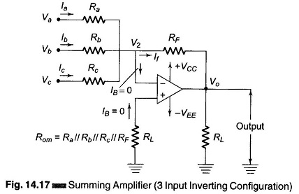
Using Kirchoff‘s circuit equation, we have la + lb + lc = IB + If. But IB ≡ 0 and V1 ≡ V2 ≡ 0
Therefore
![]()
i.e.
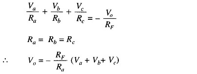
In this circuit Ra = Rb = Rc = RF.
Therefore
![]()
Hence the output voltage is the negative sum of all the input voltages. If each input voltages is amplified by a different factor, i.e. weighted differently at the output, the circuit is called a scaling or weighted amplifier (Fig. 14.17). The condition can be obtained by making Ra, Rb, and Rc, different in value. The output voltage of the scaling amplifier is then
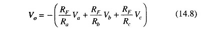
where RF/Ra ≠ RF/Rb ≠ RF/Rc.
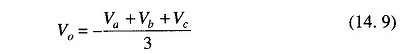
Figure 14.17 can be modified to be used as an average amplifier. In this amplifier, the output voltage is the average value of the input voltages. This modification can be obtained by making Ra = Rb = Rc = R. Also, the gain by which input is amplified must be equal to 1 over the number of inputs, i.e. RF/R = 1/n where n is the number of inputs. Therefore the output voltage is given by Vo = Va + Vb + Vc.
Therefore the output voltage for three inputs is RF/R = 1/3. The output voltage is given by