SCR Control Circuit Diagram:
Pulse Control – The simplest of SCR Control Circuit Diagram is shown in Fig. 19-8(a). If SCR1 was an ordinary rectifier, the ac supply voltage would be half- wave rectified and only the positive half-cycles would appear across the load (RL). The same would be true if the SCR gate had a continuous bias voltage to keep it on when the anode-cathode voltage goes positive. A trigger pulse applied to the gate can switch the device on at any time during the positive half-cycle of the supply voltage. The SCR continues to conduct during the rest of the positive half-cycle, and then it switches off when the instantaneous level of the supply approaches zero. The resultant load waveform is a portion of the positive half-cycle commencing at the instant that the SCR is triggered [Fig. 19-8(b)]. Resistor RG holds the gate-cathode voltage at zero when no trigger input is present.
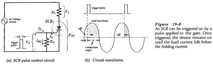
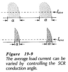
Load waveforms that result from the SCR being switched on at different points in the positive half-cycle of the supply voltage are shown in Fig. 19-9. It is seen that the average load current is controlled by the SCR conduction angle. Thus, the load power dissipation can be varied by adjusting the SCR switch-on point. It should be noted that the SCR cannot be triggered precisely at the 0° point in the waveform, because the anode-to-cathode voltage must be at lease equal to the forward on voltage (VTM) for the device. Also, the SCR will switch off before the 90° point when the load current falls below the holding current.
The instantaneous level of the load voltage is the instantaneous supply voltage (es) minus the SCR forward voltage (VTM);
![]()
The load current can be calculated from VL and RL, apd the instantaneous supply voltage (es(o)) that causes the SCR to switch off can be determined from VTM, RL, and the holding current:
![]()
For any given application, the selected SCR must have forward and reverse blocking voltages greater that the peak supply voltage. Its specified maximum rms current must also be greater than the rms load current. When designing the circuit, the gate current used should be at least three times the specified IG for the device.
Note that the required triggering current (IT) for the circuit in Fig. 19-8 is the sum of IG and the resistor current IRG, as illustrated.
90° Phase Control:
In the 90° phase-control circuit shown in Fig. 19-11, the gate triggering voltage is derived from the ac supply via resistors R1, R2, and R3. When the moving contact is set to the top of R2, the SCR can be triggered on almost immediately at the commencement of the positive half-cycle of the input. When the moving contact is set to the bottom of R2, the SCR might not switch on until the peak of the positive half-cycle. Between these two extremes, the device can be switched on somewhere between the zero level and the peak of the positive half-cycle, (between 0° and 90°). If the triggering voltage (VT) is not large enough to trigger the SCR at 90°, then the device will not trigger on at all, because VT is greatest at the supply voltage peak and falls off past the peak
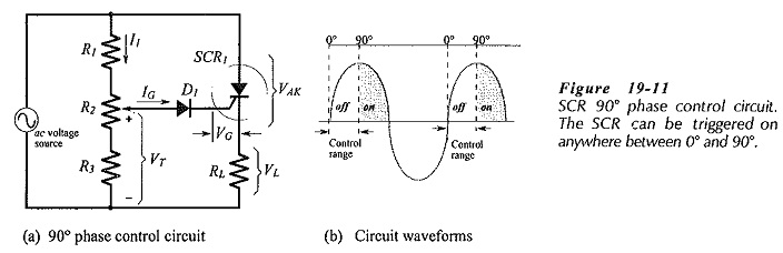
Diode D1 in Fig. 19-11 is included in the circuit to protect the SCR gate from the negative voltage that would otherwise be applied to it during the negative half-cycle of the ac supply.
The load for an SCR Control Circuit Diagram could be a permanent magnet motor, so that the circuit controls the motor speed. Alternatively, the load might be a heater or a light, and in this case the circuit controls the heater temperature or the light intensity.
The voltage divider (R1 R2 R3) in Fig. 19-11 is designed in the usual way for the required range of adjustment of VT. The voltage divider current (I1) is selected much larger than the SCR gate current. The instantaneous triggering voltage at switch-on is,
![]()
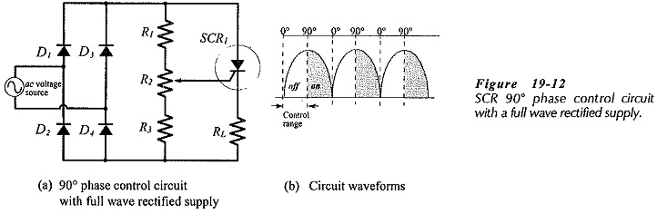
Figure 19-12 shows a 90° phase control circuit with its ac voltage source full-wave rectified. This gives a larger maximum power dissipation in the load than a non-rectified source. Also, diode D1 in Fig. 19-11 is not required in Fig. 19-12 because the SCR gate does not become reverse biased.
In the circuit in Fig. 19-13(a) the two SCRs are connected in inverse-parallel and they operate independently as 90° phase control circuits. SCR1 controls the load current during the positive half-cycle of the supply voltage, and SCR2 controls the current during the negative half-cycle. The triggering voltage for each SCR is set by the voltage divider network R1 through R4 and adjusted by variable resistor R3. Diodes D1 and D2 protect the gate terminals of each SCR from excessive reverse voltage.
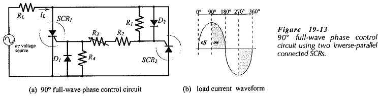
During the supply voltage positive half-cycle, D2 is forward biased and current flows through R2, R3, and R4. The voltage drop across R4, triggers SCR1 at the desired point in the positive half cycle. When triggered, the SCR forward voltage switches to a low level, and remains there until the instantaneous supply voltage level approaches zero. During the supply negative half-cycle, D1 is forward biased to produce current flow through R1, R2, and R3. With R1 equal to R4, the voltage drop across R1 triggers SCR2 at the same point in the negative half-cycle as SCR1 in the positive half-cycle. The resultant 90° full-wave phase controlled load waveform is shown in Fig. 19-13(b).
180° Phase Control:
In the circuit shown in Fig. 19-15, resistor R1 and capacitor C1 determine the point in the supply voltage cycle where the SCR switches on. During the negative half-cycle of the supply, C1 is charged via diode D1 to the negative peak of the supply voltage. When the negative peak is passed, D1 is reverse biased because its anode (connected to C1) is more negative than its cathode. With D1 reversed, C1 commences to discharge via R1. While C1 voltage remains negatively, D2 is reverse biased and the gate voltage cannot go positive to trigger the SCR on. Depending on the values of C1 and R1, the capacitor might be completely discharged at the beginning of the positive half-cycle of the supply; allowing SCR1, to switch on. Alternatively, C1 might retain some negative charge past the end of positive half-cycle; keeping SCR1 off. Resistor R2 is included in the circuit to restrict the level of the gate current.
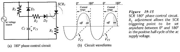
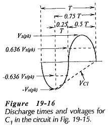
Design of the 180° phase control circuit can commence with selection of a capacitor much larger than stray capacitance. A maximum resistance for R1 should then be calculated to discharge the capacitor voltage to zero during the time from the negative peak of the supply voltage to the 180° point in the positive half-cycle. The capacitor voltage does not decrease linearly as Fig. 19-16 implies. However, the maximum resistance for R1 can be most easily calculated by assuming a linear discharge. The average value of the discharging voltage (E) is first determined. Figure 19-16 shows that E is -0.636 Vs(pk) for 0.25 T, and +0.636 Vs(pk) for 0.5 T, which averages out to approximately 0.2 Vs(pk) for the total discharge time of 0.75 T. Now the equation for discharge of a capacitor to zero volts via a resistor may be applied.
![]()
Substituting the appropriate quantities into the equation gives,