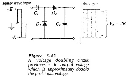
Voltage Doubler Circuit:
A Voltage Doubler Circuit produces an output voltage which is approximately double the peak voltage of the input waveform. Consideration of the voltage doubler circuit diagram in Fig. 3-42 shows that it is simply a combination of two diode-capacitor clamping circuits without the discharge resistors. In fact, the circuit operation is similar to that of clamping circuits.
When the input voltage is negative, as shown in Fig. 3-43(a), diode D1 is forward biased, and C1 charges to (E – VF1) with the polarity illustrated. D2 is reverse biased during the negative half-cycle of the input, so the charge on C2 Is not affected at this time.
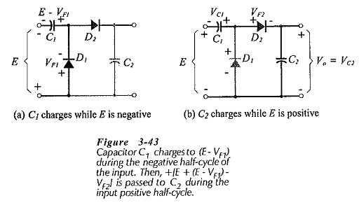
Figure 3-43(b) shows what occurs during the input positive half-cycle. D1 is now reverse biased, and D2 is forward biased. The voltage applied to D2 and C2 is the sum of the input voltage and the voltage on C1. So, as illustrated, capacitor C2 is charged to,
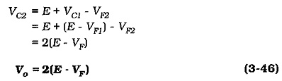
It is seen that, when the diode voltage drop is much smaller than the input voltage, the output is approximately double the peak input amplitude. The polarity of the output voltage can be reversed by reversing the polarity of the diodes and capacitors.
The output terminals of the Voltage Doubler Circuit are the terminals of capacitor C2. The load current partially discharges the capacitors, producing an output voltage drop in the same way that tilt is created on a clamping circuit output. The repeated charge and discharge of C1 and C2 results in a ripple waveform on the output.
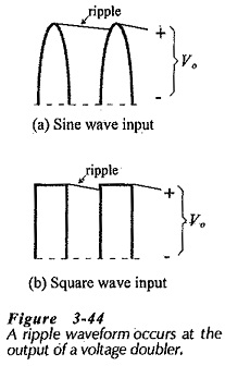
A sinusoidal input waveform to a Voltage Doubler Circuit produces exactly the same type of output ripple that occurs with a half-wave rectifier, [Fig. 3-44(a)]. However, the input most often used is a dc voltage source which has been chopped, or converted into a square waveform, [Fig. 3-44(b)].
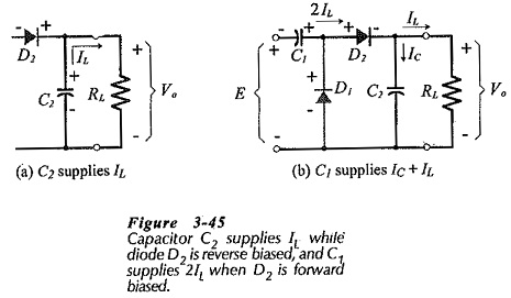
Capacitor C2 supplies the load current (IL) while diode D2 is reverse biased, [Fig. 3-45(a)]. The discharge of C2 accounts for half the output ripple voltage amplitude, and the discharge of C1 produces the other half of the ripple amplitude. Equation 3-43 can be modified for calculating the capacitance of C2.
While D2 is forward biased [Fig. 3-45(b)], capacitor C1 supplies IL and the recharging current to C2. The recharging current must equal IL to maintain the full charge on C2, so C1 supplies 2IL. Applying Eq. 3-43 to calculate C1, it is found that,
![]()
Four Stage DC Voltage Multiplier Circuit:
A Four Stage DC Voltage Multiplier Circuit is shown in Fig. 3-47. Comparing to the voltage doubler in Fig. 3-42, it is seen that this circuit consists of two cascade-connected voltage doubling circuits. To simplify the explanation of the circuit operation, assume ideal diodes with VF = 0.
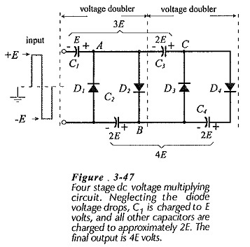
- When Vi = -E; D1 is forward biased, and C1 charges via D1 to E.
- When Vi = +E; point A is at +2E, D1 is reverse biased, D2 is forward biased, C2 charges via D2 to 2E.
- When Vi = -E; point A is close to ground level, point B is at 2E (because of VC2), D2 is reverse biased, D3 is forward biased, and C3 charges via D3 to 2E volts.
- When Vi= +E; point A is at +2E, point B is at +2E, and point C is at +4E, D4 is forward biased, and C4 charges via D4 to 2E volts.
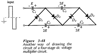
The resulting output voltage, taken across C2 and C4 is 4E volts, as illustrated. Additional stages may be added to the circuit to produce higher levels of dc output voltage. Figure 3-48 shows another way that do DC Voltage Multiplier Circuit diagrams are often drawn. Examination of the circuit shows that it is exactly the same as Fig. 3-47.