UJT Circuit Diagram:
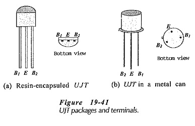
UJT Circuit Diagram Operation : The Unijunction transistor (UJT) consists of a bar of lightly-doped n-type silicon with a block of p-type material on one side, [see Fig. 19-39(a)].The end terminals of the bar are identified as Base 1 (B1) and Base 2 (B2), and the p-type block is named the emitter (E).
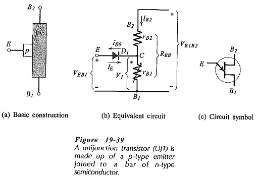
Figure 19-39(b) shows the UJT equivalent circuit. The resistance of the n-type silicon bar is represented as two resistors, rB1 from B1 to point C, and rB2 from B2 to C, as illustrated. The sum of rB1 and and rB2 is identified as RBB. The p-type emitter forms a pn-junction with the n-type silicon bar, and this junction is shown as a diode (D1) in the equivalent circuit.
With a voltage VB1B2 applied as illustrated, the voltage at the junction rB1 and rB2 is,
Note that V1 is also the voltage at the cathode of the diode; point C in the equivalent circuit.
With the emitter terminal open-circuited, the resistor current is,
If the emitter terminal is grounded, the pn-junction is reverse biased and a small emitter reverse current (IE0) flows.
Now consider what happens when the emitter voltage (VEB1) is slowly increased from zero. When VEB1 equals V1 the emitter current is zero. (With equal voltage levels on each side of the diode, neither reverse nor forward current flows.) A further increase in VEB1 forward biases the pn-junction and causes a forward current (IE) to flow from the p-type emitter into the n-type silicon bar. When this occurs, charge carriers are injected into the rB1 region. The resistance of the semiconductor material is dependent on doping, so the additional charge carriers cause the resistance of the rB1 region to rapidly decrease. The decrease in resistance reduces the voltage drop across rB1, and so the pn-junction is more heavily forward biased. This in turn results in a greater emitter current, and more charge carriers that further reduce the resistance of the rB1 region. (The process is termed regenerative) The input voltage is pulled down, and the emitter current (IE) is increased to a limit determined by the VEB1 source resistance. The device remains in this on condition until the emitter input is open-circuited, or until IE is reduced to a very low level.
The circuit symbol for a UJT Circuit Diagram is shown in Fig. 19-39(c). As always, the arrowhead points in the conventional current direction for a forward-biased junction. In this case it points from the p-type emitter to the n-type bar.
UJT Characteristics:
A plot of emitter voltage VEB1 versus emitter current IE gives the UJT emitter characteristics. Refer to the UJT Circuit Diagram terminal voltages and currents identified in Fig. 19-40(a) and to the equivalent circuit in Fig. 19-39(b). Note that when VB1B2 = 0, IB2 = 0 and V1 =0. If VEB1 is now increased from zero, the resultant plot of VEB1 and IE is simply the characteristic of a forward-biased diode with some series resistance. This is the characteristic for IB2 = 0 in Fig. 19-40(b).
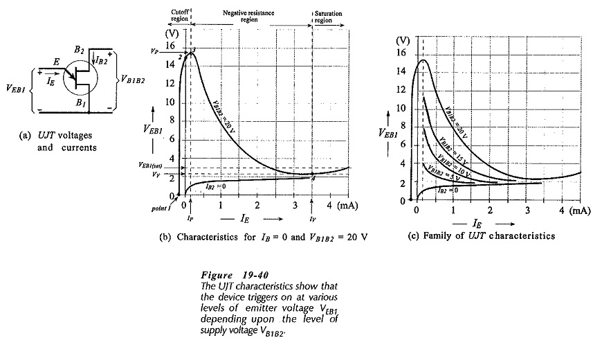
When VB1B2 is 20 V the level of V1 (Fig. 19-39(b)] might be around 15 V, depending on the resistances of rB1 and rB2. With VB1B2 = 20 V and VE = 0, the emitter junction is reverse biased and the emitter reverse current IE0 flows, as shown at point 1 on the VB1B2 = 20 V characteristic in Fig. 19-40(b). Increasing the level of VEB1 until it equals V1 gives IE = 0; point 2 on the characteristic. Further increase in VEB1 forward biases the emitter junction, and this gives the peak point on the characteristic (point 3). At the peak point, VEB1 is identified as the peak voltage (VP) and IE is termed the peak current (Ip).
Up until the peak point the UJT is said to be operating in the cutoff region of its characteristics. When VEB1 arrives at the peak voltage, charges carriers are injected from the emitter to decrease the resistance of rB1, as already explained. The device enters the negative resistance region, rB1 falls rapidly to a saturation resistance (rs), and VEB1 falls to the valley voltage (VV), [point 4 on the characteristic in Fig. 19-40(b)]. IE also increases to the valley current (IV) at this time. Further increase in IE causes the device to enter the saturation region where VE equals the sum of VD and IErS.
Starting with VB1B2 lower than 20 V gives a lower peak point voltage and a different characteristic. Thus, using various levels of VB1B2, a family of VEB1/IE characteristics can be plotted for a given UJT, as shown in Fig. 19-40(c).
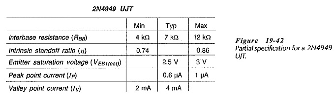
UJT Packages:
Two typical UJT packages with the terminal identified are shown in Fig 19-41. These are similar to low-power BJT packages.
UJT Parameters:
Interbase Resistance (RBB): This is the sum of rB1 and rB2 when IE is zero. Consider Fig. 19-42 that shows a portion of the manufacturer’s data sheet for 2N4949 UJT. RBB is specified as 7 kΩ typical, 4 kΩ minimum, and 12 kΩ maximum. The value of RBB, together with the maximum power dissipation PD, determine the maximum value of VB1B2 that may be used. With IE = 0,
![]()
Like all other devices, the PD of the UJT must be derated for increased temperature levels.
Intrinsic Standoff Ratio (η): The intrinsic standoff ratio is simply the ratio of rB1 to RBB. The peak point voltage is determined from η, the supply voltage, and the diode voltage drop;
![]()
Emitter Saturation Voltage (VEB1(sat)): The emitter voltage when the UJT is operating in the saturation region of its characteristics; the minimum VEB1 level. Because it is affected by the emitter current and the supply voltage, VEB1(sat) is specified for given IE and VB1B2 levels.
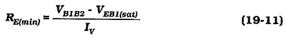
Peak Point Emitter Current (IP): IP is important as a lower limit to the emitter current. If the emitter voltage source resistance is so high that IE is not greater than IP the UJT will simply not trigger on. The maximum emitter voltage source resistance is,
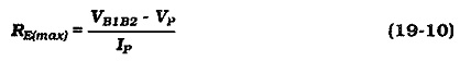
Valley Point Current (IV): IV is important in some circuits as an upper limit to the emitter current. If the emitter voltage source resistance is so low that IE is equal to or greater than IV, the UJT will remain on once it is triggered; it will not switch off. So, the minimum emitter voltage source resistance is,
UJT Relaxation Oscillator:
The relaxation oscillator circuit in Fig. 19-43(a) consists of a UJT and a capacitor (C1) charged via resistance RE. When the capacitor voltage (VC) reaches VP the UJT fires and rapidly discharges C1 to VEB1(sat). The device then cuts off and the capacitor commences charging again. The cycle is repeated continually, generating a sawtooth waveform across C1 as illustrated in Fig. 19-43(b). The time (t) for the capacitor to charge from VEB1(sat) to VP may be calculated, and the frequency of the sawtooth determined approximately as 1/t. The discharge time (tD) is difficult to calculate because the UJT is in its negative resistance region and its resistance is changing. However, tD is much less than t, and so it can normally be neglected. Rewriting Eq. 19-6,
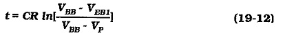
Resistor R3 in the circuit in Fig. 19-43 is included to produce a spike waveform output, as illustrated. When the UJT fires, the current surge through terminal B2 produces the negative-going voltage spike across R3. A resistor could also be included in series with terminal B1 to produce positive-going spikes. Both resistor values should be much lower than the RBB for the UJT.
UJT Control of an SCR:
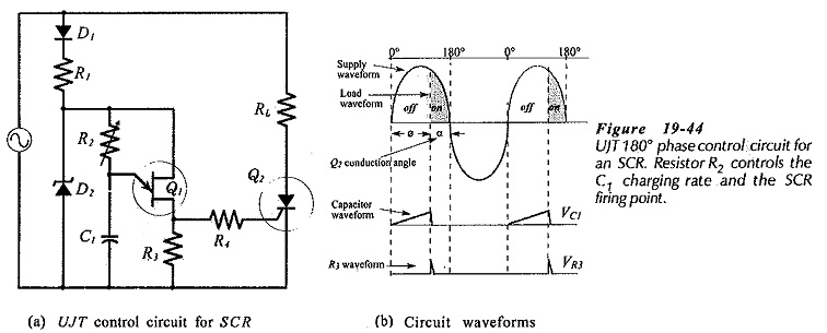
Unijunction transistors are frequently employed in SCR and TRIAC control circuits. In the typical circuit shown in Fig. 19-44(a) diode D1, resistor R1, and Zener diode D2 provide a low-voltage dc supply to the UJT circuit derived from the positive half-cycle of the ac supply voltage. D1 also isolates the UJT Circuit Diagram during the supply negative half-cycle. Capacitor C1 is charged via resistor R2 to the UJT firing voltage, and the SCR is triggered by the voltage drop across R3. By adjusting R2 the charging rate of C1 and the UJT firing time can be selected. The waveforms in Fig. 19-44(b) show that 180° of SCR phase control is possible.