Common Source Power Amplifier Using an Op Amp Driver Stage:
Basic Circuit Operation – The Class-AB MOSFET Power Amplifier with OP Amp Driver Stage circuit in Fig. 18-45(a) consists of an operational amplifier (A1), two MOSFETs (Q3 and Q4), and several resistors. The op-amp together with resistors R4, R5, and R6 and capacitor C2 constitutes a non-inverting amplifier. The two MOSFETs are a complementary Common Source Amplifier output stage.
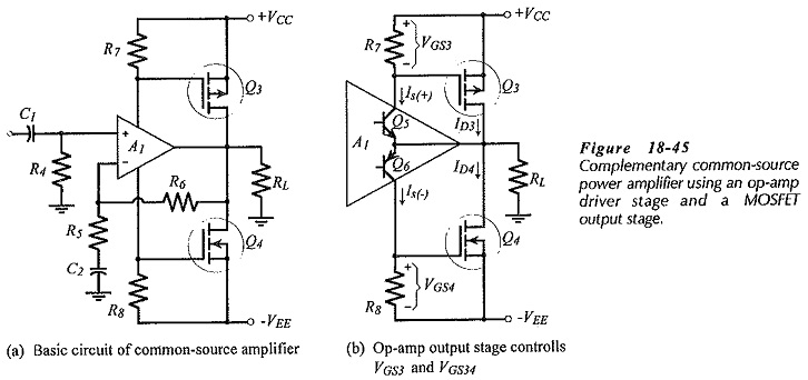
The gate-source bias voltages for Q3 and Q4 are provided by the voltage drops across resistors R7 and R8, which are in series with the op-amp supply terminals. So, the op-amp supply currents (IS(+) and IS(-)) determine the levels of VGS3 and VGS4.
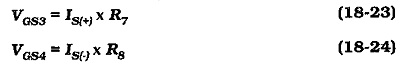
Suitable gate-source threshold voltages (VGS(th)) to bias the output transistors for Class AB operation, and typical op-amp supply currents (IS) can be determined from the device data sheets.
Figure 18-45(b) shows that the op-amp supply currents are largely the collector currents in the op-amp output stage BJTs (Q5 and Q6). Thus, R7 and R8 are collector resistors for Q5 and Q6. When the base voltage for Q5 and Q6 is increased in a positive direction, Q5 collector current (IS(+)) increases, causing VGS3 to increase, and thus increasing the MOSFET drain current ID3. At the same time, the Q6 collector current (IS(-)) decreases, reducing VGS4 and drain current ID4. The result ID3 flows through RL producing a positive output voltage swing (+Vo). Note that the op-amp output voltage is also positive at this time.
When the base voltage at Q5 and Q6 is negative-going, IS(-) increases, causing an increase in VGS4 and an increased level of ID4. During this time, IS(+) decreases, reducing VGS3 and ID3. Thus, ID4 flows through RL producing a negative output voltage swing (-Vo). The op-amp output voltage is also going negative during the time that Q4 is creating the negative output voltage across RL.
It is seen that BJTs Q5 and Q6 operate as common-emitter amplifier stages and that MOSFETs Q3 and Q4 function as Common Source Amplifier circuits. Both stages produce voltage gain which should be multiplied with the op-amp open-loop gain to determine the total open-loop gain for the circuit. Using typical quantities, the overall open-loop gain can be shown to be around 4 x 10⁶.
Returning to Fig. 18-45(a), the complete (basic) circuit operates as a non-inverting amplifier with a closed-loop voltage gain;
As explained, the power MOSFETs produce the high output current required by the amplifier load. An op-amp operating alone could not supply the load current.
Bias Control:
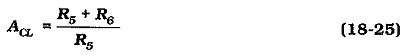
As previously discussed, the bias current in the output transistors of a MOSFET Power Amplifier with OP Amp Driver Stage should be adjustable. Control over the bias current flowing in transistor Q3 in Fig. 18-47(a) might be achieved by using a variable resistor for R7, as illustrated. This allows ID3 to be adjusted by varying VGS3. When ID3 is increased, and the additional drain current flows through RL, the dc feedback keeps the Vo equal to zero. The feedback produces the necessary change in VGS4 to make ID4 closely follow ID3. Thus, adjustment of resistor R7 controls the level of ID4 as well as ID3.
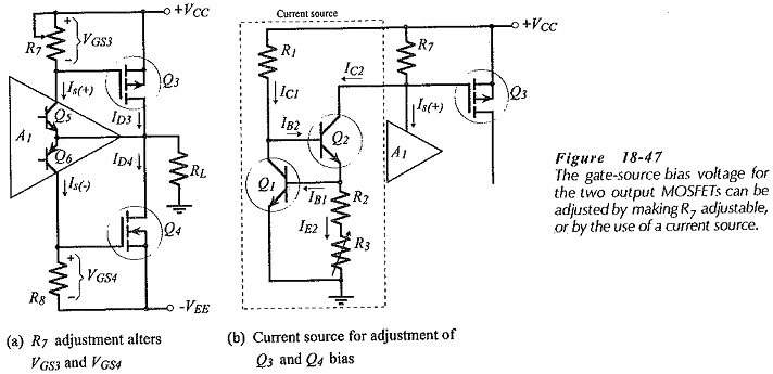
A disadvantage of using R7 to adjust the bias current is that the voltage gains produced by Q5 and Q6 become unequal when R7 and R6 have different resistance values. This can be overcome by the negative feedback, however, the bias resistors can be kept equal by using the variable current source shown in Fig. 18-47(b).
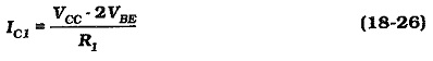
In the variable current source, transistor Q1 is biased from the emitter of Q2, and the Q2 base is connected to the collector of Q1. The collector-emitter voltage of Q1 is,![]()
Assuming that IB2 ≪ IC1, the Q1 collector current is,
With IB1 ≪ IE2, the Q2 collector current is approximately,
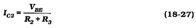
Variable resistor R3 controls the level of IC2. Also.
![]()
As explained, the dc negative feedback causes VGS4 to always be equal to VGS3, So, R3 controls the MOSFET gate-source voltages, and thus controls the quiescent drain current. The ac load offered to the collector of Q5 [see Fig. 18-45(b)] is R7, regardless of the Q2 current. Consequently, the Q5 and Q6 stage gains are equal.
Output Voltage Swing:
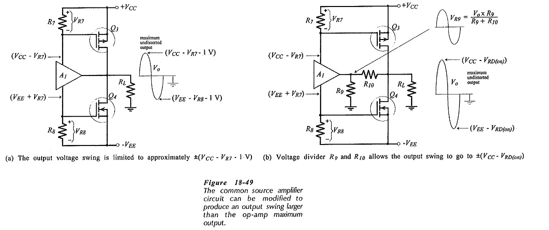
One problem with the basic circuit in Fig. 18-45 is that the output voltage swing is limited by the voltage levels at the op-amp supply terminals. As illustrated in Fig. 18-49(a), the positive supply voltage to the op-amp is (VCC – VR7), and the negative supply voltage is -(VEE – VR8). Also, recall that VR7 must be increased by ΔVGS3 in order to drive the output in a positive direction, and VRB must be increased by ΔVGS4 to drive Vo negative.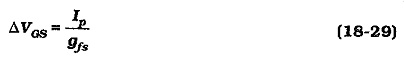
In Eq. 18-29, Ip is the peak output voltage delivered to RL and gfs is the MOSFET forward transconductance. Thus, the minimum supply voltage levels at the op-amp terminals are,
![]()
The op-amp peak output voltage is normally limited to approximately 1 V below the voltages at the supply terminals, (although, as previously noted, rail-to-rail op-amp are available). Consequently, the output voltage swing from the circuit is likely to be less than ±(VCC – 4 V), [see fig. 18-49(a)]. For greatest efficiency, it is necessary to drive the output as closely as possible to ±VCC. This can be achieved by the circuit modification shown in Fig. 18-49(b).
Resistors R9 and R10 in Fig. 18-49(b) divide Vo, so that the op-amp output can be substantially lower than the peak output voltage developed across RL. This means that the voltage levels at the op-amp supply terminals no longer limits the amplifier output voltage swing. Now, the largest peak output voltage that can be achieved is limited only by the supply voltage and RD(on).
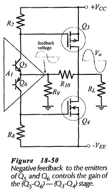
R9 and R10 also provide negative feedback that controls the gain of the stage made up of the op-amp output BJTs and the common source Amplifier. This is illustrated in Fig. 18-50. A further function of R9 and R10 is that they can be selected to limit the op-amp output current in the event of RL becoming short-circuited.
Class-AB Common Source Power Amplifier:
The complete circuit of the Common Source Power Amplifier with OP Amp Driver Stage is shown in Fig. 18-52. Note the inclusion of resistors R11 and R12, and capacitors C3 and C4. Resistors R11 and R12 are typically 100 Ω. They have no effect on the circuit dc conditions, but they help to reduce the possibility of oscillations in the output stage. The additional stage of voltage gain constituted by the MOSFETs and the op-amp (common-emitter) output transistors increases the possibility of circuit instability. Capacitor C3 helps to ensure frequency stability by acting with resistor R9 to introduce a phase lead in the output stage feedback loop. The phase lead cancels some of the phase lag in the overall circuit.
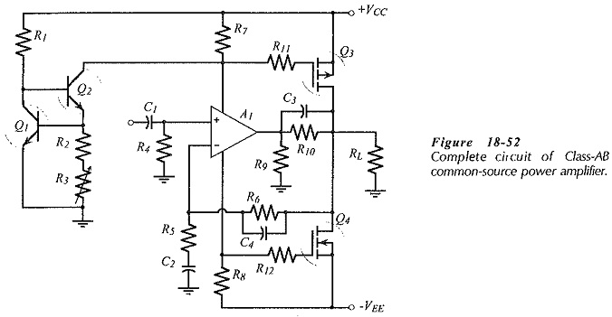
The additional stage of amplification extends the high cut-off frequency of the amplifier above the cut-off frequency of the op-amp operating alone. If the op-amp (full power) upper cutoff frequency for an overall voltage gain of 20 (or 26 dB) is 200 kHz, and the additional stage has a gain of 2 (or 6 dB), the circuit cutoff frequency is 400 kHz. For audio applications, it is normal to include capacitor C4 (see Fig. 18-52) which is usually selected to set the amplifier upper cutoff frequency around 50 kHz, or lower.