CE Transistor Characteristics:
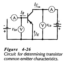
Common Emitter Circuit – Figure 4-26 shows a circuit for determining CE Transistor Characteristics. The input voltage is applied between the B and E terminals, and the output is taken at the C and E terminals. The emitter terminal is common to both input and output. Voltage and current levels are measured as shown.
Input Characteristics of Common Emitter Configuration:
To prepare a table of values for constructing the Input Characteristics of Common Emitter Configuration, VCE is held constant, VBE is set at convenient levels, and the corresponding IB levels are recorded. IB is then plotted versus VBE, as shown in Fig. 4-27. It is seen that the Input Characteristics of Common Emitter Configuration (like the common base input characteristics) are those of a forward-biased pn-junction. It should be remembered that IB is only a small portion of the total current (IE) that flows across the forward-biased BE junction.
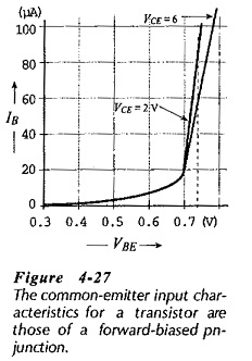
Figure 4-27 also shows that, for a given level of VBE, IB is reduced when higher VCE levels are employed. This is because higher VCE produces greater depletion region penetration into the base, reducing the distance between the CB and EB depletion regions. Consequently, more of the charge carriers from the emitter flow across the CB junction, and fewer flow out via the base terminal.
Common Emitter Output Characteristics:
To prepare a table of values for plotting the Common Emitter Output Characteristics, IB is maintained constant at several convenient levels. VCE is adjusted in steps at each IB level, and the IC level is recorded at each VCE step. For each IB level, IC is plotted versus VCE to give a family of CE Transistor Characteristics as shown in Fig. 4-28.
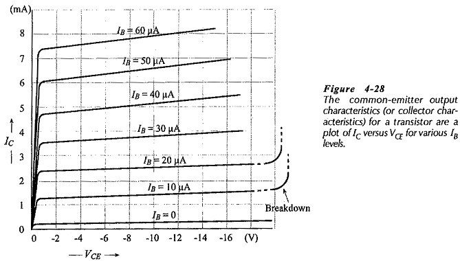
Because IE is not held constant (as it is for the common-base output characteristics) the shortening of the distance between the depletion regions (when VCB is increased) draws more charge carriers from the emitter to the collector. Thus, IC increases to some extent with increasing VCE although IB is held constant. So, the slopes of the Common Emitter Output Characteristics are much more pronounced than those of the common base characteristics.
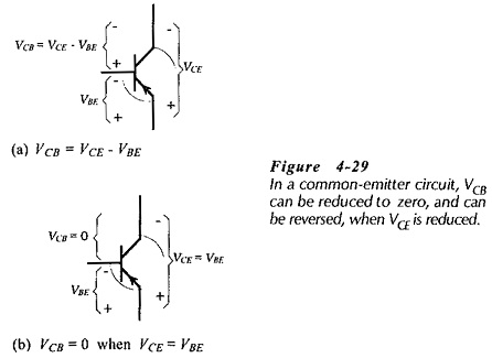
On Fig. 4-28 note that IC reduces to zero when VCE becomes zero. This is because the horizontal axis voltage is VCE, which equals (VCB + VBE), (see Fig. 4-29). At the knee of the CE Transistor Characteristics, the CB junction voltage (VCB) has been reduced to zero, (because VCE = VBE). Further reduction in VCE causes the CB junction to be forward biased. The forward bias repels the minority charge carriers, thus reducing IC to zero. The dashed lines in Fig. 4-28 show that, if VCE exceeds a maximum safe level, IC increases rapidly and the device may be destroyed. As for common-base configuration, this is due to punch-through.
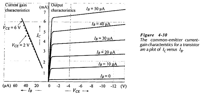
Common Emitter Current Gain Characteristics:
The Common Emitter Current Gain Characteristics are (output current) IC plotted versus (input current) IB for various fixed levels of VCE. Like the common base current gain characteristics, they can be obtained experimentally, or derived from the output characteristics. To experimentally obtain the table of IC and IB values, VCE is held at a selected level, and the base current IB Is adjusted in steps. The corresponding IC level is recorded at each step of IB.