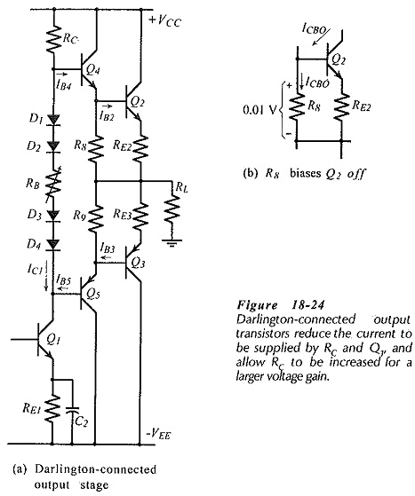
Darlington Connected Output Transistors:
High-power transistors usually have low current gains, so relatively large base currents must flow into Q2 and Q3 to supply a high load current. This means that the quiescent current through Q1 must be large, and consequently resistor RC is small. The small value of RC keeps the amplifier voltage gain low. To improve on this situation, Darlington Connected Output Transistors may be used, as illustrated in Fig. 18-24(a).
Transistors Q4 and Q5 in Fig. 18-24(a) are low-power devices that supply base current to output transistors Q2 and Q3, respectively. Note the four biasing diodes in Fig. 18-24(a) to bias the four transistor base-emitter junctions.
When peak load current (Ip) flows, the peak base current to Q4 and Q5 is,
This reduced base current allows IRC(min) to be smaller, giving a larger resistance for RC, and resulting in a larger voltage gain.
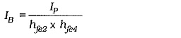
Resistors R8 and R9 in Fig. 18-24(a) are included to bias Q2 and Q3 off when Q4 and Q5 are in cutoff. The largest possible resistance values should normally be selected for R8 and R9. When Q2 and Q3 are off, the collector-base leakage current ICBO flows in R8 and R9, [see Fig. 18-24(b)],
The voltage drop across the resistors (ICBO R8) should be much smaller than the normal transistor base-emitter voltage. Selecting ICBO R8 equal to 0.01 V normally gives satisfactory resistor values. R8 and R9 are not required when power Darlington Connected Output Transistors are used.