Reverse Bias PN Junction:
When an external bias voltage is applied to a pn-junction, positive to the n-side and negative to the pride, electrons from the n-side are attracted to the positive terminal, and holes from the p-side are attracted to the negative terminal. As shown in Fig. 1-21, holes on the p-side of the junction are attracted away from the junction, and electrons are attracted away from the junction on the n-side. This causes the depletion region to be widened and the barrier voltage to be increased, as illustrated. With the barrier voltage increase there is no possibility of majority charge carrier current flow across the junction, and the junction is said to be Reverse Bias PN Junction. Because only a very small reverse current flows, a Reverse Bias PN Junction can be said to have a high resistance.
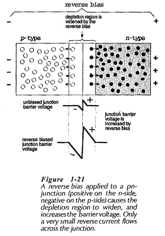
Although there is no possibility of a majority charge carrier current flowing across a Reverse Bias PN Junction, minority carriers generated on each side can still cross the junction.
Electrons in the p-side are attracted across the junction to the positive voltage on the n-side. Holes on the n-side may flow across to the negative voltage on the p-side. This is shown by the junction reverse characteristic, or the graph of reverse current (IR) versus reverse voltage (VR), (Fig. 1-22).
vi Characteristics of Reverse Bias:
Only a very small reverse bias voltage is necessary to direct all available minority carriers across the junction, and further increases in bias voltage do not increase the current. This current is referred to as a Reverse Saturation Current.
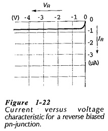
The reverse saturation current is normally a very small quantity, ranging from nanoamps to microamps, depending on the junction area, temperature, and semiconductor material.