Optocoupler Circuit Operation:
An Optocoupler Circuit Operation (optoelectronic coupler) is essentially a photo-transistor and an LED combined in one package. Figure 20-35(a) and (b) shows the typical circuit and terminal arrangement for one such device contained in a DIL plastic package. When current flows in the LED, the emitted light is directed to the phototransistor, producing current flow in the transistor. The coupler may be operated as a switch, in which case both the LED and the phototransistor are normally off. A pulse of current through the LED causes the transistor to be switched on for the duration of the pulse. Linear signal coupling is also possible. Because the coupling is optical, there is a high degree of electrical isolation between the input and output terminals, and so the term optoisolator is sometimes used. The output (detector) stage has no effect on the input, and the electrical isolation allows a low-voltage dc source to control high voltage circuits.
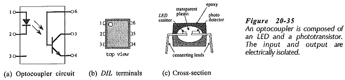
The cross-section diagram in Fig. 20-35(c) illustrates the construction of an optocoupler. The emitter and detector are contained in a transparent insulating material that allows the passage of illumination while maintaining electrical isolation.
Specification:
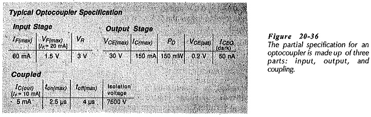
The partial specification for an optoelectronic coupler in Fig. 20-36 has three parts. The first part specifies the current and voltage conditions for the input (LED) stage. The second deals with the output (phototransistor) stage. The third part defines the coupling parameters. The transistor collector current is listed as 5 mA (typical) when its VCE = 10 V and the LED has IF = 10 mA. In this particular case, the ratio of output current to input current is 50%. This is known as the current transfer ratio (CTR), and for an optoelectronic coupler with a transistor output it can range from 10% to 150%.
Applications:
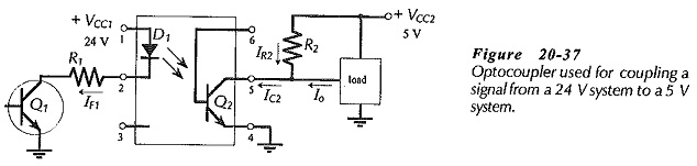
The Optocoupler Circuit Operation in a dc or pulse-type coupling application is shown in Fig. 20-37. The diode current is switched on and off by the action of transistor Q1 operating from a 24 V supply. Transistor Q2 is turned on into saturation when D1 is energized. The collector current of Q2 provides the load (sinking) current and the current through resistor R2. Pull-up resistor R2 is necessary to ensure that the load terminal is held at the 5 V supply level when Q2 is off.
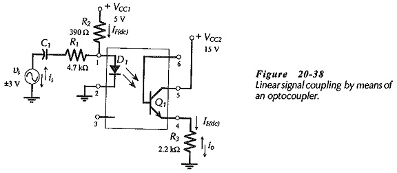
A linear application of an Optocoupler Circuit Operation is shown in Fig. 20-38. The 5 V supply provides a dc bias current to D1 via R2, and the ac signal coupled via C1 and R1 increases and decreases the diode current. Transistor Q1 is biased into an on state by the direct current through D1, and its emitter current is increased and decreased by the variation in light level produced by the alternating current in D1. An output voltage is developed across R3.
Other Optocouplers:
Other types of optocouplers involve different types of output stage. The three types illustrated in Fig. 20-39 are; (a) Darlington-output type, (b) SCE-output, and (c) TRIAC-output. In (a), the photodarlington output stage provides much higher CTR than a BJT phototransistor output stage (typically 500%), but it also has a slower response lime. The output stages in (b) and (c) are a light-activated SCR and a light-activated TRIAC, respectively. They are used with the kind of control circuits, where high electrical isolation between the triggering circuit and the control device is an additional requirement. CTR does not apply to SCR and TRIAD output stages; instead, the LED current needed to trigger the thyristor is of interest.
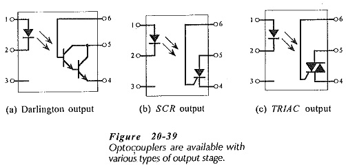
Optocoupler output stages are not designed for high load currents. Maximum current levels for Darlington outputs are around 150 mA, and 300 mA is typical for SCR and TRIAC outputs. When high load currents are to be switched, the optocoupler output stage is used as a trigger circuit for a high power device.