Impatt Diode Working:
IMPATT Diode Working is a combination of delay involved in generating avalanche current multiplication, together with delay due to transit time through a drift space, provides the necessary 180° phase difference between applied voltage and the resulting current in an Impatt Diode Working. The cross section of the active region of this device is shown in Figure 12-28. Note that it is a diode, the junction being between the p+ and the it layers.
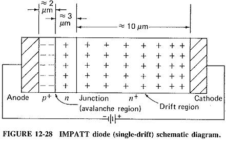
An extremely high voltage gradient is applied to the Impatt Diode Working, of the order of 400 kV/cm, eventually resulting in a very high current. A normal diode would very quickly break down under these conditions, but the IMPATT diode is constructed so as to be able to withstand such conditions repeatedly. For example, a normal diode breaks down under avalanche conditions because of the enormous powers generated. Consider that the thickness of an IMPATT diode’s active region is a few micrometers, to ensure the correct transit time for microwave operation. Its cross-sectional area is similarly tiny, to ensure a small capacitance. With the high-voltage gradient and resulting high current, the power being generated is of the order of 100 MW/cm3. The delay between the proposal for the IMPATT diode and its first realization was due in no small measure to the problems involved in dissipating such vast amounts of heat. This had to be done, to ensure a satisfactorily low operating temperature for the Impatt Diode Working, so that it would not be destroyed by melting. Typical operating temperatures of commercial diodes are of the order of 250°C. Such a high potential gradient, back-biasing the diode, causes a flow of minority carriers across the junction. If it is now assumed that oscillations exist, we may consider the effect of a positive swing of the RF voltage superimposed on top of the high dc voltage.
Electron and hole velocity has now become so high that these carriers form additional holes and electrons by knocking them out of the crystal structure, by so-called impact ionization. These additional carriers continue the process at the junction, and it now snowballs into an avalanche. If the original dc field was just at the threshold of allowing this situation to develop, this voltage will be exceeded during the whole of the positive RF cycle, and avalanche current multiplication will be taking place during this entire time. Since it is a multiplication process, avalanche is not instantaneous. As shown in Figure 12-28, the process takes a time such that the current pulse maximum, at the junction, occurs at the instant when the RE voltage across the diode is zero and going negative. A 90° phase difference between voltage and current has been obtained.
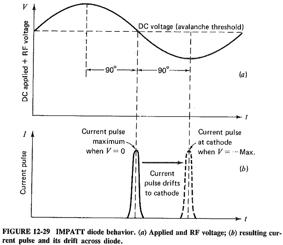
The current pulse in the Impatt Diode Working is situated at the junction. However, it does not stay there. Because of the reverse bias, the current pulse flows to the cathode, at a drift velocity dependent on the presence of the high dc field. The time taken by the pulse to reach the cathode depends on this velocity and of course on the thickness of the highly doped (n+) layer. The thickness of the drift region is cunningly selected so that the time taken for the current pulse to arrive at the cathode corresponds to a further 90° phase difference. As shown in Figure 12-29, when the current pulse actually arrives at the cathode terminal, the RF voltage there is at its negative peak. Voltage and current in the IMPATT diode are 180° out of phase, and a dynamic RF negative resistance has been proved to exist. Such a negative resistance lends itself to use in oscillators or amplifiers. Because of the short times involved, these can be microwave. Note that the device thickness determines the transit time, to which the IMPATT diode is very sensitive. Unlike the Gunn diode, the IMPATT diode is essentially a narrowband device (especially when used in an amplifier).
Practical considerations:
Commercial IMPATT diodes have been available for quite some time. They are made of either silicon, gallium arsenide or even indium phosphide. The diodes are mostly mesa, and epitaxial growth is used for at least part of the chip; some have Schottky barrier junctions. Gallium arsenide is theoretically preferable and should give lower noise, higher efficiencies and higher maximum operating frequencies. However, silicon is cheaper and easier to fabricate. Accordingly, silicon IMPATT diodes, which came first, are even now preferred for many applications; indeed, it is silicon diodes that currently provide the highest output powers at the highest operating frequencies (in excess of 200 GHz).
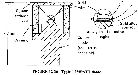
The Impatt Diode Working shown in Figure 12-30 is a typical commercial diode for use below about 50 GHz and could house either a GaAs or an Si chip. At higher frequencies, beam-lead packages almost identical in appearance to those shown in Figure 12-5 tend to be preferred. The construction is deceptively simple. However, a lot of thought and development has gone into its manufacture, particularly the contacts, which must have extremely low ohmic and thermal resistance. Additionally, in a practical circuit, the IMPATT diode is generally embedded in the wall of a cavity, which then acts as an external heat sink.
Until a few years ago, practical IMPATT diodes were unlike Read’s original proposal. This called for a double-drift region, whereas Figures 12-28 and 12-30 show diodes with single- (n+) drift regions. The reason for the initial departure from what was theoretically a higher-efficiency structure was difficulty in fabrication, but this problem has now been solved. For some years IMPATT diodes with two drift regions (one n+ and the other p+) have been made commercially. In the manufacturing process, an n layer is epitaxially grown on an n+ substrate. The p layer is then grown epitaxially or by ion implantation, and finally the p+ layer is formed by diffusion. These p+ -p-n-n+ devices were at first known as RIMPATT (Read-IMPATT) diodes, but they are now commonly known as double-drift IMPATT diodes. They are undoubtedly the versions used at the highest frequencies and for the highest output powers.