Forward and Reverse Bias Characteristics of Diode:
Figures 2-4 and 2-5 show typical Forward and Reverse Bias Characteristics of Diode for low-current silicon and germanium diodes. From the silicon diode characteristics in Fig. 2-4, it is seen that the forward current (IF) remains very low (less than microamps) until the diode forward-bias voltage (VF) exceeds approximately 0.7 V. Above 0.7 V, IF increases almost linearly with increase in VF.
Forward and Reverse Bias Characteristics of Silicon Diode:
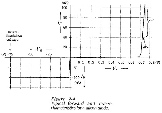
Because the diode reverse current (IR) is very much smaller than its forward current, the reverse characteristics are plotted with expanded current scales. For a silicon diode, IR is normally less than 100 nA, and it is almost completely independent of the reverse-bias voltage. As already explained, IR is largely a minority charge carrier reverse saturation current. A small increase in IR can occur with increasing reverse-bias voltage, due to some minority charge carriers leaking along the junction surface. For a diode with the characteristics in Fig. 2-4, the reverse current is typically less than 1/10,000 of the lowest normal forward current level. Therefore, IR is quite negligible when compared to IF, and a reverse-biased diode may be treated almost as an open switch.
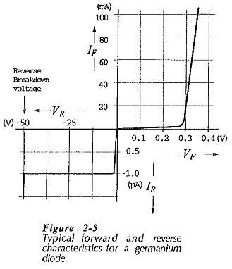
Forward and Reverse Bias Characteristics of Germanium Diode:
When the diode reverse voltage (VR) is sufficiently increased, the device goes into reverse breakdown. For the characteristics shown in Fig. 2-4, reverse breakdown occurs at 75 V. Reverse breakdown can destroy a diode unless the current is limited by a suitable series-connected resistor. Reverse breakdown is usefully applied in Zener diodes.
The Forward and Reverse Bias Characteristics of Germanium Diode are similar to those of a silicon diode, with some important differences. The forward voltage drop of a germanium diode is typically 0.3 V, compared to 0.7 V for silicon. For a germanium device, the reverse saturation current at 25°C may be around 1 μA, which is much larger than the reverse current for a silicon diode. Finally, the reverse breakdown voltage for germanium devices is likely to be substantially lower than that for silicon devices.
The lower forward voltage drop for germanium diodes can be a distinct advantage. However, the lower reverse current and higher reverse breakdown voltage of silicon diodes make them preferable to germanium devices for most applications.
Ideality Factor of Diode:
The diode parameters of greatest interest are:
- VF – forward voltage drop
- IR – reverse saturation current
- VBR – reverse breakdown voltage
- rd – dynamic resistance
- IF(max) – maximum forward current
The values of these quantities are normally listed on the diode data sheet provided by device manufacturers. Some of the parameters can be determined directly from the Forward and Reverse Bias Characteristics of Diode. For the silicon diode characteristics in Fig. 2-4, VF ≈ 0.7 V, IR = 100 nA, and VBR = 75 V.
The forward resistance is a static quantity; it is a constant resistance ,of the diode at a particular constant forward current. The dynamic resistance of the diode is the resistance offered to changing levels of forward voltage. The dynamic resistance, also known as the incremental resistance or ac resistance, is the reciprocal of the slope of the forward characteristics beyond the knee. Referring to Fig. 2-4, and Fig 2-7,
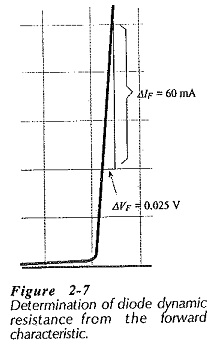
The dynamic resistance can also be calculate from the equation, 26
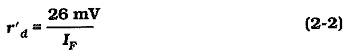
where IF is the dc forward current at the junction. Thus, for example, the dynamic resistance for a diode passing a 10 mA forward current is, r’d = 26 mV/10 mA = 26 Ω.
Equation 2-2 shows that the diode dynamic resistance changes with the level of dc forward current. This is not shown in Figs. 2-4 and 2-5, so, the characteristics are approximations of the actual device characteristics. It should also be noted that Eq. 2-2 gives the ac resistance only for the junction. It does not include the dc resistance of the semiconductor material, which might be as large as 2 Ω depending on the design of the device. The resistance derived from the slope of the device characteristic does include the semiconductor dec resistance. So, rd (from the characteristic) should be slightly larger than r’d calculated from Eq. 2-2.