Commutating Capacitor in Bistable Multivibrator or Speed up Capacitor:
Commutating Capacitor in Bistable Multivibrator is also called as Speed up Capacitor. Whenever a triggering pulse is applied to change the bistable state from one bistable state to another, it is necessary that the transition period should be minimum and it should require minimum but finite amount of energy. First requirement of the triggering process is to bring the transistors into active region i.e., the cut-off and the saturated transistors operating point should be shifted to active region. For expedition of this process, it is necessary that the closed-loop gain should be much more than unity during the transition phase. By connecting capacitors of picofarad range across R1 and R2, this objective can be achieved.
For transient they act as short circuit, and increases the regenerative feedback gain by bypassing the resistor across which the respective capacitor is connected. Secondly these capacitors supply the excess charge in the base, required to bring the off transistor to active region.
Similarly to turn off a transistor, the excess charge stored in the base region is to be withdrawn. The capacitors achieve this objective as well, if the value is appropriately chosen.
Such capacitors, which assist in transfer of conduction from one transistor to another, are known as Commutating Capacitor in Bistable Multivibrator or Speed up Capacitor.
Some of the switching times associated with the state-change-over process are defined below:
Resolution Time: It is defined as the minimum time interval between the triggers to which the binary will respond. If the duration between the triggering pulses is less than the resolution time then the binary will not function properly. The reciprocal of the resolution time is the maximum operating frequency of the binary. Resolution time comprises of transition time and the settling time.
Transition Time: It is defined as the time duration after the application of trigger pulse, during which the conduction is transferred from the off transistor to the on transistor. The commutating capacitor reduces the transition time by (i) increasing the closed-loop gain during the transient phase by acting as short circuit, (ii) by supplying the required excess charge to the base of off transistor by impulsive current flow at the instant of triggering and (iii) by withdrawing the excess charge from the base of the saturated transistor so as to reduce the storage time.
It has been further observed that the transition time can also be reduced by the trigger pulse duration slightly in excess of the minimum duration required.
Settling Time: Once the transfer of conduction from one transistor to another is over i.e., transition phase is complete, the voltages of the commutating capacitors must also change corresponding to the other stable state. Thus, the additional time required to complete the charge of the commutating capacitors after the completion of the commutation process is known as settling time.
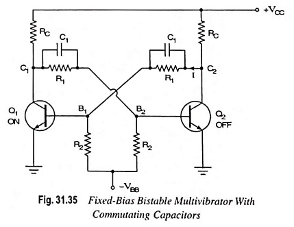
Let us assume that when the power supply is switched on, Q1 is turned on and Q2 is off. Let now a negative pulse of short duration and sufficient magnitude be applied to the base of transistor Q1. This reduces the forward bias on the transistor Q1 and causes a reduction in collector current and, thereby, increase in potential of its collector terminal C1. For proper operation this rising voltage is to be transmitted to the base of Q2 without delay.
The build-up time of VC1 is negligible but the build-up time of base voltage of transistor Q2 i.e., VB2 is determined by time constant R′C′ where R′ is the parallel combination of R1 and R2 and C′ is the input capacitance of transistor Q2 (without commutating capacitor C1). The build-up time of VB2 may be improved by connecting Commutating Capacitor in Bistable Multivibrator C1 across resistors R1, as shown in Fig. 31.35. It acts as a compensated attenuator formed by R1, C1, R2, C′. If the capacitor C1 is of large value, the buildup time of VB2 can be as small as that of VC1. Thus, full amplitude of rise of VC1 is transmitted to VB2 without delay. However, the value of speed-up capacitor C1 is restricted because of resolution time. Too small value of Commutating Capacitor in Bistable Multivibrator results in large transition time whereas too large value of commutating capacitor results in longer settline time. So, a compromise is to be made.
The maximum frequency of operation is given as

The resolution time of bistable multivibrator can be improved by
- Reducing all stray capacitances or junction capacitances. By doing so, charging time can be reduced.
- Reducing the values of R1, R2 and RC Reduction in the values of R1 and R2 will reduce the charging time of speed-up capacitors resulting in improvement in transition speed. Reduction in the values of resistors also reduces the recovery time.
- By not allowing the transistors to go into saturation. This will reduce the storage time resulting in fast change from on to off state.