Digital Integrated Circuits

Synchronous Sequential Circuits

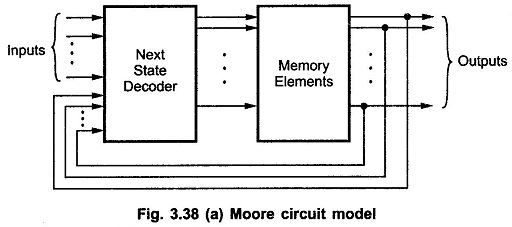
Synchronous Sequential Circuits or Clocked Sequential Circuits: In Synchronous Sequential Circuits or clocked sequential circuits, clocked flip-flops are used as memory elements, which change their individual states in synchronism with the periodic clock signal. Therefore, the change in states of flip-flops and change in state of the entire circuit occurs at the transition of the […]

Synchronous Sequential Circuits Read More »

Performance of CMOS Gates

Performance of CMOS Gates: The Performance of CMOS Gates which based on following different categories namely, Operating Speed : Slower than TTL series. Approximately 25 to 100 ns depending on the subfamily of CMOS Inverter Circuit. It also depends on the power supply voltage. Voltage Levels and Noise Margins : The voltage levels for CMOS

Performance of CMOS Gates Read More »

CMOS NOR Gate Circuit

CMOS NOR Gate Circuit: Fig. 3.4 shows 2-input CMOS NOR Gate Circuit. Here, P-channel MOSFETs Q1 and Q2 are connected in series and N-channel MOSFETs Q3 and Q4 are connected in parallel. Like NAND circuit, this circuit can be analyzed by realizing that a LOW at any input turns ON its corresponding P-channel MOSFET and turns OFF

CMOS NOR Gate Circuit Read More »

CMOS NAND Gate Circuit Diagram

CMOS NAND Gate Circuit Diagram: Fig. 3.3 shows CMOS NAND Gate Circuit Diagram 2-input NAND gate. It consists of two P-channel MOSFETs, Q1 and Q2, connected in parallel and two N-channel MOSFETs, Q3 and Q4 connected in series. P-channel MOSFET is ON when its gate voltage is negative with respect to its source whereas N-channel

CMOS NAND Gate Circuit Diagram Read More »

Parallel Adder and Subtractor

Parallel Adder and Subtractor: Parallel Adder and Subtractor which consists of three categories, namely,    n Bit Parallel Adder,Binary Parallel Adder and n Bit Parallel Subtractor. n Bit Parallel Adder: We have seen, a single full-adder is capable of adding two one-bit numbers and an input carry. In order to add binary numbers with more

Parallel Adder and Subtractor Read More »

Half Adder and Full Adder Circuit

Half Adder and Full Adder Circuit: Adders are divided into two categories namely, half adder and full adder circuit. Half Adder Circuit: The Half Adder Circuit operation needs two binary inputs : augend and addend bits; and two binary outputs : sum and carry. The half adder truth table shown in 3.6 gives the relation

Half Adder and Full Adder Circuit Read More »

Programmable Array Logic (PAL)

Programmable Array Logic (PAL)

Programmable Array Logic (PAL): We have seen that PLA device with a Programmable AND array and Programmable OR array. However, Programmable Array Logic (PAL) is a programmable logic device with a fixed OR array and a programmable AND array. Because only AND gates are programmable , the PAL is easier to program, but is not

Programmable Array Logic (PAL) Read More »

Programmable Logic Array (PLA)

Block Diagram of Programmable Logic Array

Programmable Logic Array (PLA) | Block Diagram of PLA: The combinational circuit do not use all the minterms every time. Occasionally, they have don’t care conditions. Don’t care condition when implemented with a ROM becomes an address input that will never occur. The result is that not all the bit patterns available in the ROM

Programmable Logic Array (PLA) Read More »

Read Only Memory (ROM)

Read Only Memory (ROM): A Read Only Memory (ROM) is a device that includes both the decoder and the OR gates within a single IC package. The Fig. 3.82 shows the block diagram of ROM. It consists of n input lines and m output lines. Each bit combination of the input variables is called an

Read Only Memory (ROM) Read More »

Scroll to Top