Modulation and Demodulation

Generation of DSBSC Signal using Balanced and Ring Modulator

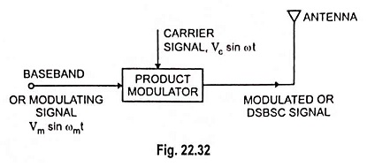
Generation of DSBSC Signal using Balanced and Ring Modulator: DSBSC signal can be obtained by simply multiplying the modulating signal with the carrier signal. By simple multiplication of Vc sin ωct and Vm sin ωmt, we have the lower and upper sidebands without carrier as shown below: It means that a DSBSC signal is obtained by simply multiplying …

Generation of DSBSC Signal using Balanced and Ring Modulator Read More »

Square Law Diode Modulator – Circuit Diagram and its V-I Characteristics

Square Law Diode Modulator – Circuit Diagram and its V-I Characteristics: Basic circuit of a square law diode modulator is shown in Fig. 22.30. It utilizes the nonlinear region of voltage-current dynamic characteristic of a P-N diode. This square law diode modulator method is suited at low voltage levels because of the fact that current-voltage …

Square Law Diode Modulator – Circuit Diagram and its V-I Characteristics Read More »

Emitter Modulation – Circuit Diagram and its Operation

Emitter Modulation – Circuit Diagram and its Operation: The circuit for emitter modulation is shown in Fig. 22.29. It is essentially a CE amplifier. The carrier signal from a crystal oscillator is coupled to the base of amplifier through capacitor Cin. The modulating signal is applied to the emitter circuit. The capacitors Cin and CC are …

Emitter Modulation – Circuit Diagram and its Operation Read More »

Base Modulation Circuit Working Principle

Base Modulation Circuit Working Principle: The circuit for base modulation is shown in Fig. 22.28. The carrier signal from a crystal oscillator is coupled to the base terminal of the amplifier through transformer T1. The modulating signal is applied across resistor R1 through capacitor C1. The capacitor C1 allows only audio frequency ac signal to …

Base Modulation Circuit Working Principle Read More »

Collector Modulation Circuit – Working, Advantages and Disadvantages

Collector Modulation Circuit – Working, Advantages and Disadvantages: This is very popular method for AM generation. The circuit diagram for collector modulation is shown in Fig. 22.26. Here, the transistor Q1 makes an RF class C amplifier. The carrier signal is applied to the base of Q1. VCC makes collector supply used for biasing purpose. …

Collector Modulation Circuit – Working, Advantages and Disadvantages Read More »

Signal Definition and Classification of Signals

Signal Definition and Classification of Signals: A signal is a single valued function of one or more variables that conveys some information. Signals are represented mathematically as the functions of one or more independent variables. A signal may be a function of time, temperature, position, pressure, distance etc. In electrical sense, the signal can be …

Signal Definition and Classification of Signals Read More »

Modulation – Definition, Types and Need for Modulation

Modulation – Definition, Types and Need for Modulation: Any wave has three significant characteristics viz. amplitude, frequency and phase, and modulation is a process of impressing information to be transmitted on a high frequency wave, called the carrier wave, by changing its one of the characteristics (amplitude, frequency or phase angle). Modulation may also be …

Modulation – Definition, Types and Need for Modulation Read More »

Scroll to Top