Voltage Multiplier Circuits:
Cascaded Voltage Multiplier Circuits for higher voltages are cumbersome and require too many supply and isolating transformers. It is possible to generate very high d.c. voltages from single supply transformers by extending the simple voltage doubler circuits. This is simple and compact when the load current requirement is less than one milliampere, such as for cathode ray tubes, etc. Valve type pulses generators may be used instead of conventional a.c. supply and the circuit becomes compact. A typical circuit of this form is shown in Fig. 6.4a.
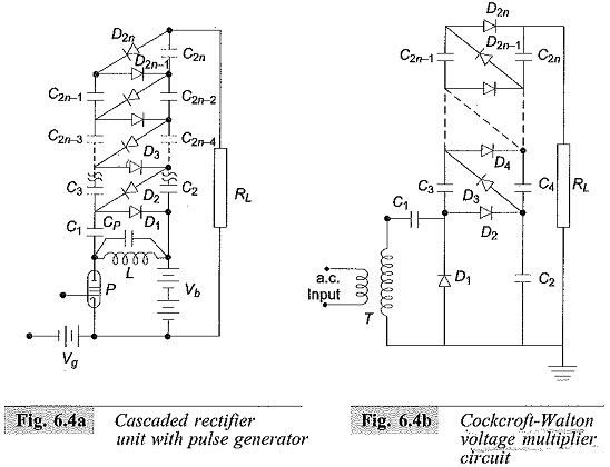
The pulses generated in the anode circuit of the valve P are rectified and the voltage is cascaded to give an output of 2nVmax across the load RL. A trigger voltage pulse of triangular waveform (ramp) is given to make the valve switched on and off. Thus a voltage across the coil L is produced and is equal to Vmax = I√L/CP, where CP is the stray capacitance across the coil of inductance L. A d.c. power supply of about 500 V applied to the pulse generator, is sufficient to generate a high voltage d.c. of 50 to 100 kV with suitable number of stages.
The pulse frequency is high (about 500 to 1000 Hz) and the ripple is quite low (<1%). The voltage drop on load is about 5% for load currents of about 150 μA. The voltage drops rapidly at high load currents.
Voltage Multiplier Circuits using the Cockcroft-Walton principle is shown in Fig. 6.4b. The first stage, i.e. D1,D2,C1,C2, and the transformer T are identical as in the voltage doubler shown in Fig. 6.3. For higher output voltage of 4, 6, … 2n of the input voltage V, the Voltage Multiplier Circuits is repeated with cascade or series connection. Thus, the capacitor C4 is charged to 4Vmax and C2n to 2nVmax above the earth potential. But the voltage across any individual capacitor or rectifier is only 2Vmax.
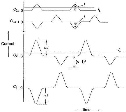
The rectifiers D1,D3, …D2n-1 shown in Fig. 6.4b operate and conduct during the positive half cycles while the rectifiers D2,D4,…D2n conduct during the negative half cycles. Typical current and voltage waveforms of such a circuit are shown in Figs 6.4c and 6.4d respectively. The voltage on C2 is the sum of the input a.c. voltage, Vac and the voltage across condenser C1,Vc1 as shown in Fig. 6.4.
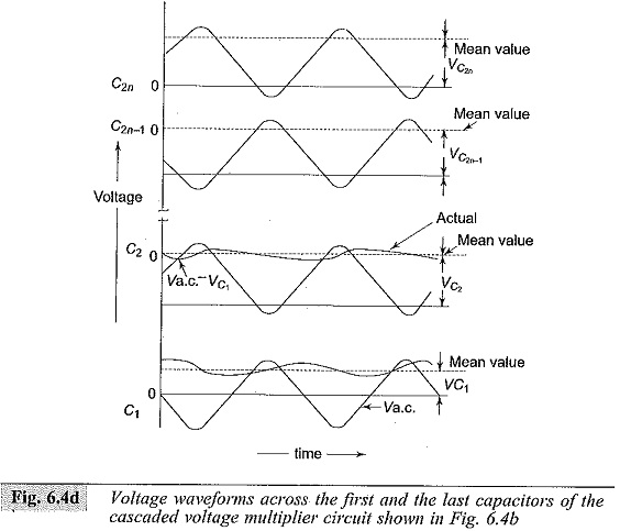
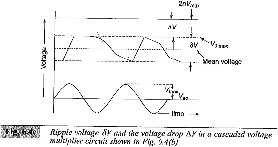
The mean voltage on C2 is less than the positive peak charging voltage (Vac + Vc1). The voltage across other capacitors C2 to C2n can be derived in the same manner (i.e.) from the difference between voltage across the previous capacitor and the charging voltage. Finally the voltage after 2n stages will be Vac (n1 + n2 + …), where n1, n2, … are factors when ripple and regulation are considered in the next rectifier. The ripple voltage δV and the voltage drop ΔV in a cascaded Voltage Multiplier Circuits unit are shown in Fig. 6.4e.
Ripple in Cascaded Voltage Multiplier Circuits:
With load, the output voltage of the cascaded rectifiers is less than 2nVmax, where n is the number of stages. The ripple and the voltage regulation of the rectifier circuit may be estimated as follows.
Let
- f = supply frequency,
- q = charge transferred in each cycle,
- I1 =load current from the rectifier,
- t1 = conduction period of the rectifiers,
- t2 = non-conduction period of rectifiers, and
- δV = ripple voltage (peak to peak)
Referring to Fig: 6.3a, when load current I1 is supplied from capacitor C2 to load RL during the non-conducting period, the charge transferred per cycle from the capacitor C2 to the load during the non-conduction period t2 is q, and is related as follows.![]()
Since t1 ≪ t2 and t1 + t2 = 1/f (i.e. the period of the a.c. supply voltage),
Hence
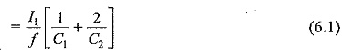
At the same time a charge q is transferred from C1 to C2 during each cycle equal to I1/fC2. Thus the total voltage drop that occurs will be I1/fC1 + 2I1/fC2. Hence, regulation = mean voltage drop from 2Vmax
Therefore, the mean output voltage
![]()
For the cascade circuit, on no load, the voltages between stages are raised by 2Vmax giving an output voltage of 2nVmax for n stages.
Referring to Fig. 6.4b, to find and expression for the total ripple voltage, let it be assumed that all capacitances C1,C2,…,C2n be equal to C. Let q be the charge transferred from C2n to the load per cycle.
Then the ripple at the capacitor C2n will be I1/fC.
Simultaneously, C2n-2 transfers as charge q to the load and to C2n-1.
Hence, the ripple at the capacitor C2n-2 is 2I1/fC.
Similarly, C2n-4 transfers a charge q to the load, to C2n-3, and to C2n-2.
Therefore, the ripple at capacitor C2n-4 is 3I1/fC.
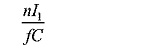
Proceeding in the same way, the ripple at C2 will be nI1/fC.
Hence, for n stages the total ripple (peak to peak) will be
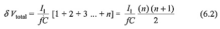
and the average ripple
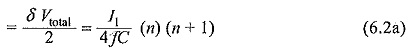
The major contribution to the ripple is from the lowest or ground end capacitors, C1,C2,C3,C4, etc. Ripple can be reduced if the capacitance of these capacitors is increased proportionately i.e., C1,C2 are made nC,C3,C4 are made (n – 1) C and so on so that the total ripple will be equal to