FET Datasheet Specifications:
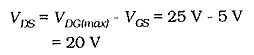
Maximum Ratings – A portion of a FET Datasheet Specifications is reproduced in Fig. 9-17. As with other device data sheets, a device type number and brief description is usually given at the start. Maximum ratings follow, and then the electrical characteristics are stated for specific bias conditions. From Fig. 9-17, the maximum drain-source voltage (VDS) for the 2N5457 through 2N5459 devices is 25 V, and the maximum drain-gate voltage (VDG) is also 25 V. This means, for example, that if a -5 V gate-source bias is used, the drain source voltage should not exceed,
Note on Fig. 9-17 that the maximum reverse gate-source voltage (VG(r)) is specified as 25 V. This is considerably greater than the (typically 5 V) maximum base-emitter reverse voltage for a BJT.
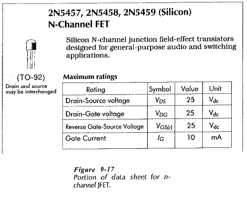
No maximum drain current is specified in Fig. 9-17, but this can be calculated from the maximum power dissipation and the VDS level. The specified gate current (IG) is the maximum gate current if the gate-channel junctions become forward biased.
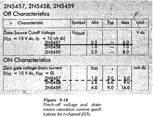
Saturation Current and Pinch off voltage:
The drain-source saturation current (IDSS) and the pinch-off voltage (VP or VGS(off)) have already been discussed. Values for these are listed in the FET Datasheet Specifications portion showing the Off Characteristics and ON Characteristics in Fig. 9-18. It is seen that VGS(off) for a 2N5457 (underlined) ranges from a minimum of 0.5 V to a maximum of 6 V. Also, the IDSS level for a 2N5457 (dashed underline) is a minimum of 1 mA and a maximum of 5 mA.
The FET transfer characteristic approximately follows the equation,
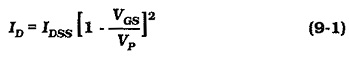
When IDSS and VP are known, a table of corresponding values of ID and VGS can be determined from Eq. 9-1. These may be used to construct the FET transfer characteristic. Because of the wide range of specified values for IDSS and VP, the transfer characteristic can differ substantially from one device to another one having the same type number. This creates a problem in FET bias circuits.
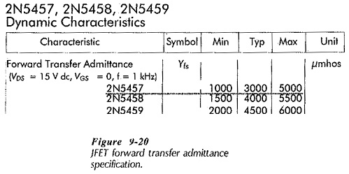
Forward Transfer Admittance:
The forward transfer admittance (Yfs) [also known as the transconductance (gm or gFS)] for a FET defines how the drain current is controlled by the gate-source voltage.
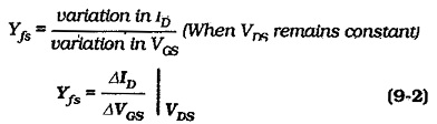
The units used for Yfs are microSiemens (μS), which can be restated as microamps per volt (μA/V). MilliSiemens (mS), or milliamps/volt (mA/V) might also be used. For a FET with Yjs = 2 mA/V. ID changes by 2 mA when VGS is altered by 1 V. In the portion of a FET Datasheet Specifications in Fig. 9-20, the Yfs units are μmhos. The mho (ohm written backwards) is another (older) name for the Siemen, the unit of conductance. For the 2N5457 (underlined) the value of YfS is specified as a minimum of 1000 μmhos, and a maximum of 5000 μmhos. An inverted ohm symbol is also sometimes used instead of the Siemens symbol.
Because Yfs defines the relationship between ID and VGS, it can be determined from the slope of the FET transfer characteristic. This is illustrated in Fig. 9-21.
The transfer characteristic for a FET Datasheet Specifications is defined by Eq. 9-1, and Yfs is determined from the slope of the transfer characteristic. So, an equation for Yfs can be derived by differentiating Eq. 9-1.
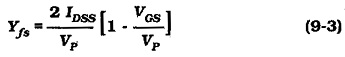
Equation 9-3 may be used to calculate the value of Yfs for any VGS level. As in Eq. 9-1, the negative sign for VGS is already included, so that only the numerical value should be entered.
Output Admittance:
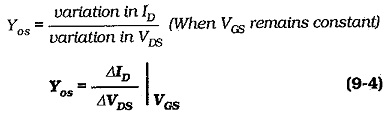
The drain resistance (rd) of a FET is the ac resistance between drain and source terminals when the device is operating in the pinch-off region of its drain characteristics. it is also the slope of the drain characteristics in the pinch-off region; (see Fig. 9-22). The drain characteristics are almost flat, so, rd is not easily determined from the characteristic. Because rd is usually the output resistance of the FET at the drain terminal, it may also be expressed as an output admittance (Yos = 1/rd).
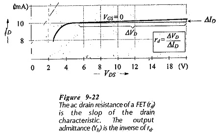
The output admittance is defined as,
Drain-Source ON Resistance:
The drain-source ON resistance (rDS(on)) (also designated RD(on)), is a dc quantity, not to be confused with the ac drain-source resistance (rds). rDS(on) is the resistance of the FET channel when the depletion regions are absent; when the device is biased ON in the channel ohmic region of the drain characteristics. (see Fig. 9-23). In this condition, the voltage drop along the channel from drain to source is ID x rDS(on)). This is the drain-source ON voltage (VDS(on)). which is similar to the VCE(sat) of a BJT.
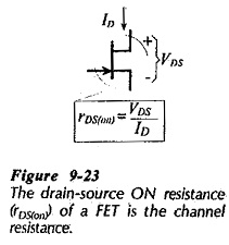
The drain-source ON resistance might typically be 60 Ω or lower. It can be an important quantity for FETs used in switching circuits. VDS(on) can be much smaller than VCE(sat) making FET gates superior to BJT gates for some applications.
Gate Cutoff Current and Input Resistance:
The gate-channel junctions in a JFET are pn-junctions, and because they are normally reverse biased, a minority charge carrier current flows. This is the gate-source cutoff current (IGSS), or gate reverse current. [see Fig. 9-24(a)). For a 2N5457 FET. IGSS is specified as 1 nA at 25°C, and 200 nA at 100°C.
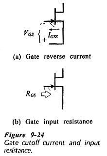
The gate input resistance (RGS) is the resistance of the reverse-biased gate-channel junctions [Fig. 9-24(b)], and it is inversely proportional to IGSS. Typical values of RGS for a JFET are 109 Ω at 25°C and 107 Ω at 100°C.
Breakdown Voltage:
The are several ways used for expressing JFET breakdown voltage. BVDGO is the drain-gate breakdown voltage with the source terminal open-circuited. BVGSS is the gate-source breakdown voltage with the drain terminal shorted to the source. Both are a specification of the voltage at which the gate-channel junctions might break down.
Noise Figure:
A FET usually has a much lower level of thermal noise than a BJT. This is because there are very few charge carriers crossing junctions in a FET. As in the case of a BJT, the FET noise figure (NF) is specified as a spot noise figure at a particular frequency and bias conditions, and for a given resistance at the input. The figure varies if any of these conditions are altered. Noise calculations for a FET circuit are performed exactly as for a BJT circuit.
Capacitances:
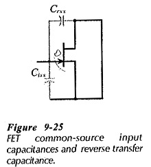
Terminal capacitances for FETs may be specified as gate-drain capacitance (Cgd). gate-source capacitance (Cgs), and drain-source capacitance (Cds). The input capacitance is sometimes expressed as the common-source input capacitance (Ciss or Cgss). This is the gate-source capacitance measured with the drain terminal shorted to the source, (Fig. 9-25). In this case, a reverse transfer capacitance (Crss) is also specified: Crss being another term for Cgd. These quantities are very important for FET high-frequency and switching circuits.