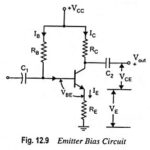
Emitter Bias Circuit Diagram
Emitter Bias Circuit Diagram: This Emitter Bias Circuit Diagram is obtained by simply introducing an emitter resistor to the fixed bias circuit as shown in Fig. 12.9. For analysis, we…
Continue Reading
Emitter Bias Circuit Diagram