Phototransistor Working:
A Phototransistor Working is similar to an ordinary BJT except that its collector base junction is constructed like a photodiode. Instead of a base current, the input to the transistor is in the form of illumination at the junction.
Construction and Working of Phototransistor:
Consider an ordinary BJT with its base terminal open-circuited, [Fig. 20-27(a)]. The collector base leakage current (ICBO) acts as a base current, giving a collector current; IC = (hFE + 1) ICBO. In the case of the photodiode, it was shown that the reverse saturation current is increased by the light energy at the junction. Similarly, in the phototransistor ICBO is proportional to the collector-base illumination, [Fig. 20-27(b)]. This results in IC also being proportional to the illumination level.
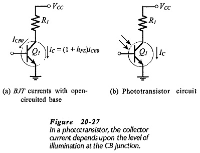
For a given amount of illumination on a very small area, the Phototransistor Working provides a much larger output current than that available from a photodiode. Thus, the phototransistor is the most sensitive of the two devices. The phototransistor circuit symbol shows a base terminal, and this is often left unconnected, but is sometime used to provide stable bias conditions.
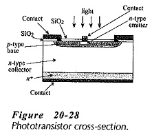
The cross-section in Fig. 20-28 illustrates the Construction and Working of Phototransistor. The emitter area is seen to be quite small, to allow incident illumination to pass to the collector-base junction. Phototransistor packages are similar to the photodiode packages, except that three terminals are provided.
Phototransistor Characteristics and Phototransistor Specifications:
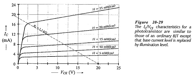
Typical output phototransistor characteristics are shown in Fig. 20-29. These are seen to be similar to BJT characteristics except that the base current levels are replaced with illumination levels. A do load line can be drawn on the characteristics in the usual way.
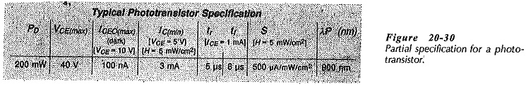
The partial Phototransistor Specifications is shown in F g. 20-30 shows a 3 mA minimum current at 5 mW/cm2, and a sensitivity of 500 μA/mW/cm2. Comparing this to the photodiode specification (Fig. 20-29) shows (as stated above) that a phototransistor is very much more sensitive than a photodiode. However, the rise and fall times (typically 5 μs and 8 μs) for a phototransistor are very much slower than the 2 ns response time for a photodiode.
Phototransistor Applications:
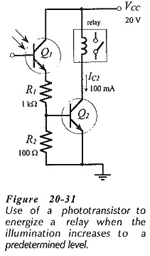
Two Phototransistor Applications are shown in Fig. 20-31 and 20-32. The relay in Fig. 20-31 is energized when the incident light on the phototransistor is raised to a particular level. This occurs when the Q1 emitter current produces sufficient voltage drop across R2 to forward bias the BE junction of Q2. The relay current falls again when Q2 turns off as the light level decreases.
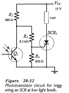
In Fig. 20-32, SCR1 remains untriggered while the illumination keeps Q1 in saturation. If the light fails, Q1 turns off and VR3 triggers the SCR on. This kind of circuit can be used to switch on an emergency lighting system when the normal lighting fails.