Phototransistor Construction and Working Principle:
The sensitivity of a photo diode can be increased by as much as 100 times by adding a junction, resulting in an NPN device. A simple representation of the Phototransistor Construction is shown in Fig. 13.36.
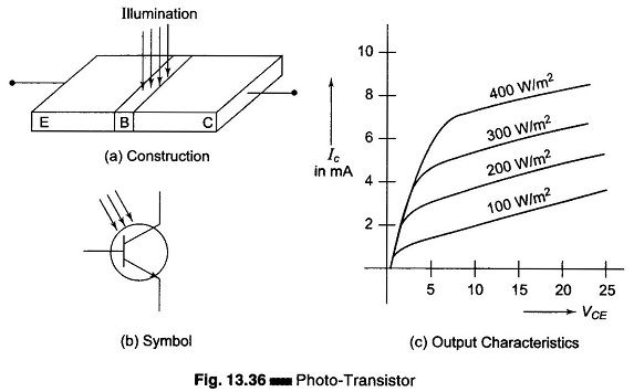
Illumination of the central region causes the release of electron hole pairs. This lowers the barrier potential across both junctions, causing an increase in the flow of electrons from the left region into the centre region and on to the right region.
For a given amount of illumination on a very small area, the phototransistor provides a much larger output current than that available from a photo diode, i.e. a photo-transistor is more sensitive.
Arrays of transistors and low current photo diodes are widely used as photo detectors for such applications as punched card and tape readouts. Photo-transistors are more sensitive than photo-diodes, but the latter have a faster switching time.
One application of a phototransistor is shown in Fig. 13.37.
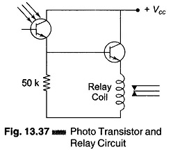
The light incident on the photo-transistor causes its current to increase and therefore increases both the voltage drop across 50 kΩ and the input to the transistor which drives the relay. This raises the current to the operational level.