Thyristors in Electronic Devices and Circuits

Programmable Unijunction Transistor

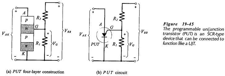
Programmable Unijunction Transistor: PUT Operation – The Programmable Unijunction Transistor (PUT) is actually an SCR-type device used to simulate a UJT. The interbase resistance (RBB) and the intrinsic standoff ratio (η) can be programmed to any desired values by selecting two resistors. This means that the device Ming voltage (the peak voltage VP) can also […]

Programmable Unijunction Transistor Read More »

UJT Circuit Diagram

UJT Circuit Diagram: UJT Circuit Diagram Operation : The Unijunction transistor (UJT) consists of a bar of lightly-doped n-type silicon with a block of p-type material on one side, [see Fig. 19-39(a)].The end terminals of the bar are identified as Base 1 (B1) and Base 2 (B2), and the p-type block is named the emitter

UJT Circuit Diagram Read More »

Silicon Bilateral Switch

Silicon Bilateral Switch: It might be convenient to think of a Silicon Bilateral Switch (SBS) as an SUS with a gate terminal, or as a low-current TRIAC. However, the SBS is not simply another four-layer device. Silicon bilateral switches are actually integrated circuits constructed of matched transistors, diodes, and resistors. This produces better parameter stability than

Silicon Bilateral Switch Read More »

Silicon Unilateral Switch

Silicon Unilateral Switch: The Silicon Unilateral Switch (SUS), also known as a four layer diode and as a Schokley diode, can be treated as a low-current SCR without a gate terminal. Figure 19-30 shows the Silicon Unilateral Switch circuit symbol and typical forward characteristics. The device triggers into conduction when a forward switching voltage (VS)

Silicon Unilateral Switch Read More »

TRIAC Control Circuit Diagram

TRIAC Control Circuit Diagram: A TRIAC Control Circuit Diagram that allows approximately 180° of phase control is shown in Fig. 19-27(a). The waveforms in Fig. 19-27(b) illustrate the circuit operation. With the TRIAC (Q1) off at the beginning of the supply voltage positive half-cycle, capacitor C1 is charged positively via resistors R1 and R2, as

TRIAC Control Circuit Diagram Read More »

TRIAC Operation and Characteristics

TRIAC Operation and Characteristics: The basic construction, equivalent circuit, graphic symbol and TRIAC Operation and Characteristics are shown in Fig. 19-21. The TRIAC behaves as two inverse-parallel connected SCRs with a single gate terminal. Sections n1,p2,n3, and p3, in Fig. 19-21(a) form one SCR that can be represented by transistors Q1 and Q2 in Fig. 19-21(b).

TRIAC Operation and Characteristics Read More »

SCR Applications Circuits

SCR Applications Circuits: SCR Applications Circuits : An SCR circuit is stable when it operates correctly: switching on and off only at the desired instants. Unwanted triggering (also called false triggering) can be produced by noise voltages at the gate, transient voltages at the anode terminal, or by very fast voltages changes at the anode

SCR Applications Circuits Read More »

SCR Control Circuit Diagram

SCR Control Circuit Diagram: Pulse Control – The simplest of SCR Control Circuit Diagram is shown in Fig. 19-8(a). If SCR1 was an ordinary rectifier, the ac supply voltage would be half- wave rectified and only the positive half-cycles would appear across the load (RL). The same would be true if the SCR gate had

SCR Control Circuit Diagram Read More »

Scroll to Top