TRIAC Control Circuit Diagram:
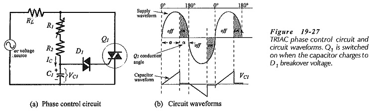
A TRIAC Control Circuit Diagram that allows approximately 180° of phase control is shown in Fig. 19-27(a). The waveforms in Fig. 19-27(b) illustrate the circuit operation. With the TRIAC (Q1) off at the beginning of the supply voltage positive half-cycle, capacitor C1 is charged positively via resistors R1 and R2, as shown. When VC1 reaches the DIAC switching voltage plus the Q1 gate triggering voltage, D1 conducts producing gate current to trigger Q1 on. C1 discharges until the discharge current falls below the D1 holding current level. The TRIAC Control Circuit Diagram switches off at the end of the supply positive half-cycle, and then the process is repeated during the supply negative half-cycle. The rate of charge of C1 is set by variable resistor R1, so that the Q1 conduction angle is controlled by adjustment of R1.
TRIAC Zero-Point Switching Circuit:
The TRIAC zero-point switching circuit in Fig. 19-28(a) produces a load waveform similar to that for the SCR zero-point circuit. The load power dissipation is controlled by switching the TRIAC on for several cycles of the supply voltage and off for several cycles, with switch-on occurring only at the negative-to-positive zero crossing point of the supply waveform, and switch-off taking place at the positive-to-negative zero point. Q1 is a low-current SCR that controls the switching point of Q2.
With switch S1 closed, Q1 is on, and the Q1 forward voltage drop is below the level required for triggering Q2, (VG2 + VD1 + VD2), [see Fig. 19-28(b)]. Thus, no gate current flows to Q2, and no conduction occurs. Q1 switches off when S1 is opened, so that IG flows to Q2 gate via C1, R2, D1, and D2 to trigger Q2 into conduction, [Fig. 19-28(c)]. With Q2 conducting, capacitor C2 is charged via D3 almost to the positive peak of the load voltage, [Fig. 19-28(d)]. The TRIAC switches off at the end of the positive half-cycle. Then, the charge on C2 (applied to the gate via D2) triggers Q2 on again just after the zero-crossing point into the negative half-cycle. (It should be noted this is quadrant IV triggering.)
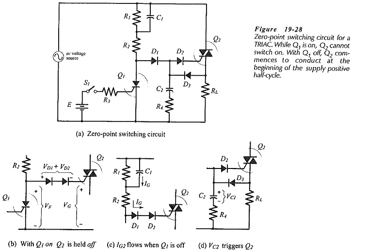
The initial Q2 switch-on occurs only at the beginning of the positive half-cycle of the supply voltage. If S1 is opened during the supply positive half-cycle, Q1 continues to conduct until the end of the half-cycle, thus keeping Q2 off. With Q2 off, C2 remains uncharged, and so it cannot trigger Q2 on during the supply negative half-cycle. Q2 triggering now occurs at the beginning of the next positive cycle.
If S1 is opened during the supply negative half-cycle, Q2 cannot be triggered into conduction, again because of the lack of charge on C2. It is seen that Q2 conduction can commence only at the beginning of the positive half-cycle of the supply voltage. Also, once triggered, Q2 conduction continues until the end of the cycle.
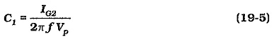
To design the circuit in Fig. 19-28, the TRIAC Control Circuit Diagram is first selected to pass the required load current and to survive the peak supply voltage. Resistor R2 is a low-resistance component calculated to limit the peak surge current to the Q2 gate in the event that the peak supply voltage is applied to the circuit without Q1 being on. Capacitor C1 has to supply triggering current (IG) to Q2 at the zero crossing point of the supply waveform when Q1 is off. Usually IG2 is selected around three times the specified IG(max) for Q2, and C1 is then calculated from the simple equation for capacitor charge; C = (I x t)/ΔV. In this case ΔV/ t can be replaced by the rate-of-change of the supply voltage at the zero crossing point, which is (2π f Vp). So, the C1 equation is,
Resistor R1 can now be determined by using the selected gate current for Q2 (IG2) as the peak anode current for Q1; R1=Vp/IG2. The Q1 gate resistor (R3) is calculated from the Q1 triggering current and the voltage of the de source; R1 =(E – VG1)/IG1.
The Q2 gate current is again used in the calculation of R4 and C2. To trigger Q2 at the start of the supply negative half-cycle, IG2 must flow from C2 into the Q2 gate, so R4 = Vp/IG2. A suitable capacitance for C2 is now calculated by again using the simple capacitance equation C2 = (IG2 x t)/ΔV. In this case, time t is selected much larger than the Q2 turn-on time, and ΔV is approximately 0.1 VP.
SCR Q1 must pass the selected anode current (IG2) and survive the peak supply voltage. The diodes must each survive the peak supply voltage and pass the Q2 triggering current,
IC Zero Voltage Switch:
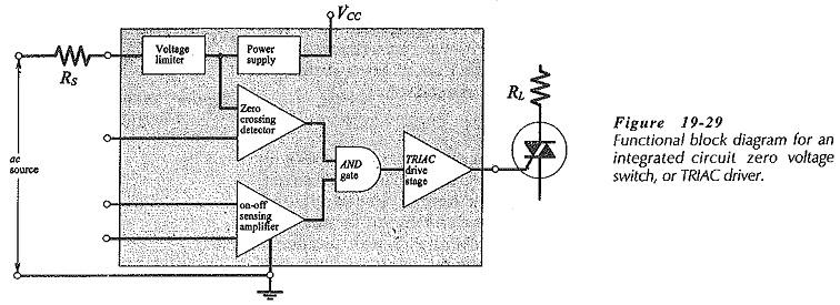
The functional block diagram for a typical Integrated circuit TRIAC driver, known as a zero voltage switch, is shown in Fig. 19-29. The device contains a voltage limiter and a dc power supply, so that it operates directly from the ac supply to the load to be controlled. There is also a zero crossing detector that provides an output pulse each time the supply waveform crosses the zero level. The zero crossing detector output is fed to an AND gate , and the AND gate output goes to the TRIAC drive stage that produces the current pulse to the TRIAC gate. An on off sensing amplifier is used to sense the voltage level from an externally-connected transducer; for example, a temperature sensing transducer would be used if the load is a heater. When the temperature drops to a predetermined level, the on-off sensing amplifier provides an input to the AND gate. The gate triggering pulse from the TRIAC drive stage occurs at the supply zero-crossing points only when the temperature is below the desired level.