Pin Diagram of Pentium Processor:
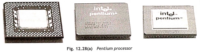
The Pentium’s memory and I/O interfaces are more advanced than the simple models. They are very different from the 8086 bus interfaces. Figure 12.28(a) shows the Pentium processor and the schematic pin diagram of Pentium processor with most signals depicted in Fig. 12.28(b). The pin functions of the Pentium processor are described below:
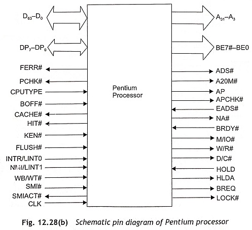
A31–A3(Output) The address bus (A31-A3) is used to drive an external memory, I/O devices and decoders. Generally, the address buses A31-A3 are used along with the byte enables signals BE7#-BE0#.
ADS#(Output) The address status signal (ADS#) shows that a new valid bus cycle is driven by the Pentium processor.
A20/M#(input) Whenever the address hit 20 mask (A20/M#) pin is asserted, the Pentium imitates the address wrap-around of the 8086. The A20/M# signal is only used in real mode.
APCHK#(Output) When the Pentium processor has detected address parity errors on an inquire or snooping cycle, the Address Parity Check (APCHK#) status signal is asserted 2 clock cycles after EADS#.
AP(Input/Output) The Address Parity (AP) signal provides an even parity information for all address cycles of Pentium processor. This signal can also be used along with APCHK# and EADS# for snooping cycles.
BE7#–BE0#(Output) The byte enable signals BE7#-BE0# are used with address buses A31-A3 to indicate the bytes which will be written to the external memory.
BF1–BF0(Input) For the duration of reset, BF1-BF0 pins are sampled and fix the ratio of the external and internal clocks.
BOFF#(Input) The Back-Off (BOFF#) input signal terminates all uncompleted bus cycles. The Pentium floats the pins normally affected by a bus hold, a clock cycle after BOFF#. When BOFF# signal is removed, the Pentium restarts all uncompleted bus cycles in their entirety.
BRDY#(Input) The Burst Ready (BRDY#) input signal is used to indicate an external device which has currently completed the read or write when BRDY#=0. If BRDY#=1, an external device needs more time. Usually this signal is sampled in the T2, T12 and T2P cycles.
BREQ(Output) The Bus Request (BREQ) output signal informs the external system that the Pentium processor has generated a bus request internally.
BUSCHK#(Input) The Bits Check (BUSCHK#) input signal allows the external system so that a bus cycle becomes unsuccessful. Therefore, a machine check exception will be generated depending on the state of CR4.
CACHE#(Output) When the Pentium processor initiates a cycle’s operation, the cache (CACHE#) output signal indicates that the current read cycle is internally cacheable. This signal is also used to indicate a burst write back cycle for a write cycle operation.
D63-D0(input/output) The 64-bit data bus of the Pin Diagram of Pentium Processor is D63-D0. D63-D56 lines are the most significant byte and D7-D0 lines are the least significant byte.
DP7-DP0 The DP7-DP0 lines are called data parity Actually, there is one bit for each byte of the data bus. For example, DP7 is used for D63-D56 and DP0 is used for D7-D0. During a write operation, the Pentium processor generates even parity in the same cycle. But during a read operation, the external system has to drive even parity back into the Pentium.
CLK(Input) The clock (CLK) input gives the fundamental timing for Pentium cycles. All timings signal except the JTAG signals are always referred to the clock input.
CLK(Input) In a single-processor based system, CPUTYPE is connected to ground. In a dual-processor based system, the primary processor’s CPUTYPE will be connected to ground and the secondary processor’s CPUTYPE must be connected to +VCC.
PCHK#(0utput) The Parity Check (PCHK#) output signal is used to indicate the result of a parity check on a specified data read.
PEN#(input) The Parity Enable (PEN#) input signal is used with CR4MCE to determine whether a machine cycle exception can be taken as a result of a parity error on a read cycle.
WR#(Dual-Input/Output) The W/R# signal is used to differentiate the read and write operations. If W/R# = 1, this signal represents a write operation. When W/R#=0, this signal represents read operations.
D/C#(Output) The D/C# output signal is used to represent data or code. If D/C# =1, this signal represents data. When D/C# =0, this signal represents a code/special cycle. Actually, D/C#=0, M/IO#=0, W/R#=1 and the BE7#-BE0# signals are used to identify the exact type of a special cycle.
M/IO#(Dual-Input/Output) The M/IO# signal is used to distinguish the memory and input/output related operations. If M/IO# =1, this signal represents memory-related operation. When M/IO# =0, this signal represents input/output device related operations.
EADS#(Input) The EADS# signal determines that a valid external address has been driven into the Pentium processor for a snooping or inquire cycle.
FLUSH#(Input) When the FLUSH# input signal becomes low, the Pentium processor writes back to memory all changed cache lines and invalidates its code and data internal caches.
HIT#(Output) The hit signal provides the result of a snooping or inquiry cycle. When HIT# is low, it indicates a hit. If HIT# is high, it indicates a miss.
HOLD(Input) The bus hold request (HOLD) is used for bus arbitration.
HLDA(Output) The bus hold acknowledges (HLDA) is used for bus arbitration. When an external bus master asserts HOLD, the Pentium processor tri-states its output and input/output lines and also asserts HLDA after completing all outstanding bus cycles. Then external bus master releases HOLD and the Pentium leaves bus hold and release HLDA.
LOCK#(0utput) When the Lock (LOCK#) is active low, the Pentium processor does not recognize HOLD request signal.
KEN#(Input) The Cache Enable (KEN#) input signal is used to verify whether the current cycle is cacheable or not cacheable.
NA#(Input) The Next Address (N/A#) input decides whether any external system is ready to accept a new address even though all the current bus cycles have not completed. This is used to speed up memory access cycles significantly.
INTR/LINT0(Input) When INTR input signal is high, it indicates a maskable interrupt request from an external device. If the IE flag is set in the EFLAG register, the processor will accept the interrupt. The LINT0 states local interrupt 0 when the on-chip APIC is used in the Pin Diagram of Pentium Processor.
NMI/LINTI(Input) NMI stands for nonmaskable interrupt. The LINT 1 states local interrupt 1 when the on-chip APIC is used in a Pin Diagram of Pentium Processor.
RESET(Input) When Reset is high, it forces the Pentium processor to start execution at a known state and all internal caches are invalidated.
SMI#(Input) If the System Management Interrupt (SMI#) input signal is low, the Pentium processor enters the system management mode.
SMIACT#(Output) When the System Management Interrupt Active (SMIACT#) output signal goes low, it indicates that the processor is in System Management Mode (SMM).
WB/WT#(Input) The Write-Back/Write-Through (WB/WT#) input signal is used to define whether a data cache line may be used as write-back (1) or write-through (0) on a line-by-line basis. This signal also decides whether a cache line is initially in the S or E state in the data cache. Usually, it is used with the PWT bit.