PN Junction Semiconductor:
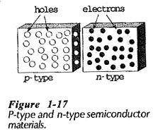
Two blocks of PN Junction Semiconductor material are represented in Fig. 1-17; one block is p-type material, and the other is n-type. The small circles in the p-type material represent holes, which are the majority charge carriers in p-type. The dots in the n-type material represent the majority charge carrier free electrons within that material. Normally, the holes are uniformly distributed throughout the volume of the p-type semiconductor, and the electrons are uniformly distributed in the n-type.
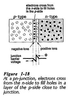
In Figure 1-18, PN Junction Semiconductor materials are shown side by side, representing a PN Junction. Holes and electrons are close together at the junction, so some free electrons from the n-side are attracted across the junction to fill adjacent holes on the p-side. They are said to diffuse across the junction from a region of high carrier concentration to one of low concentration. The free electrons crossing the junction create negative ions on the p-side by giving some atoms one more electron than their total number of protons. The electrons also leave positive ions (atoms with one fewer electron than the number of protons) behind them on the n-side.
Barrier Voltage in PN Junction:
The n-type and p-type materials are both electrically neutral before the charge carriers diffuse across the junction. When negative ions are created on the p-side, the portion of the p-side close to the junction acquires a negative voltage, (see Fig. 1-18). Similarly, the positive ions created on the n-side gives the n-side a positive voltage close to the junction. The negative voltage on the p-side tends to repel additional electrons crossing from the n-side. Also, (thinking of the holes as positive particles) the positive voltage on the n-side tends to repel any hole movement from the p-side. Thus, the initial diffusion of charge carriers creates a barrier voltage in pn junction, which is negative on the p-side and positive on the n-side. The transfer of charge carriers and the resultant creation of the barrier voltage occur when the PN Junction Semiconductor are formed during the manufacturing process.
The magnitude of the barrier voltage in pn junction Semiconductor can be calculated from a knowledge of the doping densities, electronic charge, and junction temperature. Typical barrier voltages at 25°C are 0.3 V for germanium junctions and 0.7 V for silicon.
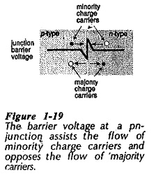
It has been explained that the barrier voltage in pn junction opposes both the flow of electrons from the n-side and the flow of holes from the p-side. Because electrons are the majority charge carriers in the n-type material, and holes are the majority charge carriers in the p-type, it is seen that the barrier voltage opposes the flow of majority carriers across the PN Junction Semiconductor, (see Fig. 1-19). Any free electrons generated by thermal energy on the p-side of the junction are attracted across the positive barrier to the n-side. Similarly. thermally generated holes on the n-side are attracted to the p-side through the negative barrier presented to them at the junction. Electrons on the p-side and holes on the n-side are minority charge carriers. Therefore, the barrier voltage assists the flow of minority carriers across the junction, (Fig. 1-19).
Depletion Region in PN Junction:
The movement of charge carriers across the junction leaves a layer on each side which is depleted of charge carriers. This is the Depletion Region in PN Junction shown in Fig. 1-20(a). On the n-side, the depletion region consists of donor impurity atoms which, having lost the free electron associated with them, have become positively charged.
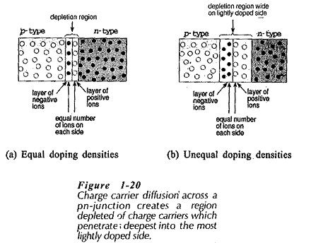
The depletion region on the p-side is made up of acceptor impurity atoms which have become negatively charged by losing the hole associated with them. (The hole has been filled by an electron.)
On each side of the junction, equal numbers of impurity atoms are involved in the depletion region. If the two blocks of PN Junction Semiconductor material have equal doping densities, the depletion layers on each side have equal widths, (Fig 1-20(a)). If the p-side is more heavily doped than the n-side, as illustrated in Fig. 1-20(b), the depletion region penetrates more deeply into the n-side in order to include an equal number of impurity atoms on each side of the junction. Conversely, when the n-side is most heavily doped, the depletion region penetrates deepest into the p-type material.