Generation of Frequency Modulation:
The Generation of Frequency Modulation system is a variable output frequency, with the variation proportional to the instantaneous amplitude of the modulating voltage. The subsidiary requirements are that the unmodulated frequency should be constant, and the deviation independent of the modulating frequency. If the system does not produce these characteristics, corrections can be introduced during the modulation process.
FM Methods:
One method of Generation of Frequency Modulation suggests itself immediately. If either the capacitance or inductance of an LC oscillator tank is varied, frequency modulation of some form will result. If this variation can be made directly proportional to the voltage supplied by the modulation circuits, true FM will be obtained.
There are several controllable electrical and electronic phenomena which provide a variation of capacitance as a result of a voltage change. There are also some in which an inductance may be similarly varied. Generally, if such a system is used, a voltage-variable reactance is placed across the tank, and the tank is tuned so that (in the absence of modulation) the oscillating frequency is equal to the desired carrier frequency, The capacitance (or inductance) of the variable element is changed with the modulating voltage, increasing (or decreasing) as the modulating voltage increases positively, and going the other way when the modulation becomes negative. The larger the departure of the modulating voltage from zero, the larger the reactance variation and therefore the frequency variation. When the modulating voltage is zero, the variable reactance will have its average value. Thus, at the carrier frequency, the oscillator inductance is tuned by its own (fixed) capacitance in parallel with the average reactance of the variable element.
There are a number of devices whose reactance can be varied by the application of voltage. The three-terminal ones include the reactance field-effect transistor (FET), the bipolar transistor and the tube. Each of them is a normal device which has been biased so as to exhibit the desired property. By far the most common of the two-terminal devices is the varactor diode. Methods of Generation of Frequency Modulation that do not depend on varying the frequency of an oscillator will be discussed under the heading “Indirect Method.” A prior generation of phase modulation is involved.
Direct Methods:
Of the various methods of providing a voltage-variable reactance which can be connected across the tank circuit of an oscillator, the most common are the reactance modulator and the varactor diode. These will now be discussed in turn.
Basic reactance modulator: Provided that certain simple conditions are met, the impedance z, as seen at the input terminals A – A of Figure 5-11, is almost entirely reactive. The circuit shown is the basic circuit of a FET reactance modulator, which behaves as a three-terminal reactance that may be connected across the tank circuit of the oscillator to be frequency-modulated. It can be made inductive or capacitive by a simple component change. The value of this reactance is proportional to the transconductance of the device, which can be made to depend on the gate bias and its variations. Note that an FET is used in the explanation here for simplicity only. Identical reasoning would apply to a bipolar transistor or a vacuum tube, or indeed to any other amplifying device.
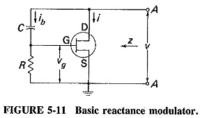
Theory of reactance modulators: In order to determine z, a voltage v is applied to the terminals A – A between which the impedance is to be measured, and the resulting current i is calculated. The applied voltage is then divided by this current, giving the impedance seen when looking into the terminals. In order for this impedance to be a pure reactance (it is capacitive here), two requirements must be fulfilled. The first is that the bias network current ib must be negligible compared to the drain current. The impedance of the bias network must be large enough to be ignored. The second requirement is that the drain-to-gate impedance (XC here) must be greater than the gate-to-source impedance (R in this case), preferably by more than 5:1. The following analysis may then be applied:
![]()
The FET drain current is

Therefore, the impedance seen at the terminals A – A is

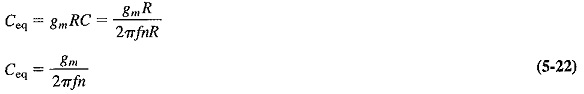
If XC ≫ R in Equation (5-17), the equation will reduce to
![]()
This impedance is quite clearly a capacitive reactance, which may be written as

From Equation (5-19) it is seen that under such conditions the input impedance of the device at A – A is a pure reactance and is given by
![]()
The following should be noted from Equation (5-20):
- This equivalent capacitance depends on the device transconductance and can therefore be varied with bias voltage.
- The capacitance can be originally adjusted to any value, within reason, by varying the components R and C.
- The expression gmRC has the correct dimensions of capacitance; R, measured in ohms, and gm, measured in siemens (s), cancel each other’s dimensions, leaving C as required.
- It was stated earlier that the gate-to-drain impedance must be much larger than the gate-to-source impedance. This is illustrated by Equation (5-17). If XC/R had not been much greater than unity, z would have had a resistive component as well.
If R is not much less than XC (in the particular reactance modulator treated), the gate voltage will no longer be exactly 90° out of phase with the applied voltage v, nor will the drain current i. Thus, the input impedance will no longer be purely reactive. As shown in Equation (5-17), the resistive component for this particular FET reactance modulator will be 1/gm. This component contains gm it will vary with the applied modulating voltage. This variable resistance (like the variable reactance) will appear directly across the tank circuit of the master oscillator, varying its Q and therefore its Output voltage. A certain amount of amplitude modulation will be created. This applies to all the forms of reactance modulator. If the situation is unavoidable, the oscillator being modulated must be followed by an amplitude limiter.
The gate-to-drain impedance is, in practice, made five to ten times the gate-to-source impedance. Let XC = nR (at the carrier frequency) in the capacitive RC reactance FET so far discussed. Then
Substituting Equation (5-21) into (5-20) gives
Equation (5-22) is a very useful formula. In practical situations the frequency of operation and the ratio of XC to R are the usual starting data from which other calculations are made.
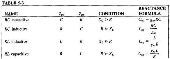
Types of reactance modulators: There are four different arrangements of the reactance modulator (including the one initially discussed) which will yield useful results. Their data are shown in Table 5-3, together with their respective prerequisites and output reactance formulas. The general prerequisite for all of them is that drain current must be much greater than bias network current. It is seen that two of the arrangements give a capacitive reactance, and the other two give an inductive reactance.
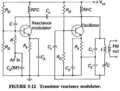
In the reactance modulator shown in Figure 5-12, an RC capacitive transistor reactance modulator, quite a common one in use, operates on the tank circuit of a Clapp-Gouriet oscillator. Provided that the correct component values are employed, any reactance modulator may be connected across the tank circuit of any LC oscillator (not crystal) with one provision: The oscillator used must not be one that requires two tuned circuits for its operation, such as the tuned-base-tuned-collector oscillator. The Hartley and Colpitts (or Clapp-Gouriet) oscillators are most commonly used, and each should be isolated.with a buffer. Note the RF chokes in the circuit shown, they are used to isolate various points of the circuit for alternating current while still providing a dc path.
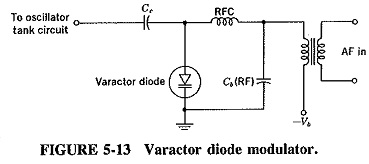
Varactor diode modulator: A varactor diode is a semiconductor diode whose junction capacitance varies linearly with the applied voltage when the diode is reverse-biased. It may also be used to produce Generation of Frequency Modulation. Varactor diodes are certainly employed frequently, together with a reactance modulator, to provide automatic frequency correction for an FM transmitter. The circuit of Figure 5-13 shows such a modulator. It is seen that the diode has been back-biased to provide the junction capacitance effect, and since this bias is varied by the modulating voltage which is in series with it, the junction capacitance will also vary, causing the oscillator frequency to change accordingly. Although this is the simplest reactance modulator circuit, it does have the disadvantage of using a two-terminal device; its applications are somewhat limited. However, it is often used for automatic frequency control and remote tuning.
Stabilized Reactance Modulator—AFC:
Although the oscillator on which a reactance modulator operates cannot be crystal-controlled, it must nevertheless have the stability of a crystal oscillator if it is to be part of a commercial transmitter. This suggests that frequency stabilisation of the reactance modulator is required, and since this is very similar to an automatic frequency control system, AFC will also be considered. The block diagram of a typical system is shown in Figure 5-14. [However, to acquire a full understanding of the operation of this circuit, it is necessary to be familiar with the phase (Foster-Seeley) discriminator, which is treated in Section 6-4.3]
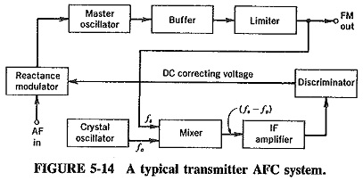
As can be seen, the reactance modulator operates on the tank circuit of an LC oscillator. It is isolated by a buffer, whose output goes through an amplitude limiter to power amplification by class C amplifiers (not shown). A fraction of the output is taken from the limiter and fed to a mixer, which also receives the signal from a crystal oscillator. The resulting difference signal, which has a frequency usually about one-twentieth of the master oscillator frequency, is amplified and fed to a phase discriminator. The output of the discriminator is connected to the reactance modulator and provides a dc voltage to correct automatically any drift in the average frequency of the master oscillator.
Operation: The time constant of the diode load of the discriminator is quite large, in the order of 100 milliseconds (100 ms). Hence the discriminator will react to slow changes in the incoming frequency but not to normal frequency changes due to Generation of Frequency Modulation (since they are too fast). Note also that the discriminator must be connected to give a positive output if the input frequency is higher than the discriminator tuned frequency, and a negative output if it is lower.
Consider what happens when the frequency of the master oscillator drifts high. A higher frequency will eventually be fed to the mixer, and since the output of the crystal oscillator may be considered as stable, a somewhat higher frequency will also be fed to the phase discriminator. Since the discriminator is tuned to the correct frequency difference which should exist between the two oscillators, and its input frequency is now somewhat higher, the output of the discriminator will be a positive dc voltage. This voltage is fed in series with the input of the reactance modulator and therefore increases its transconductance. The output capacitance of the reactance modulator is given by Ceq = gmRC, and it is, of course, increased, therefore lowering the oscillator’s center frequency. The frequency rise which caused all this activity has been corrected. When the master oscillator drifts low, a negative correcting voltage is obtained from this circuit, and the frequency of the oscillator is increased correspondingly.
This correcting dc voltage may instead be fed to a varactor diode connected across the oscillator tank and be used for AFC only. Alternatively, a system of amplifying the dc voltage and feeding it to a servomotor which is connected to a trimmer capacitor in the oscillator circuit may be used. The setting of the capacitor plates is then altered by the motor and in turn corrects the frequency.
Reasons for mixing: If it were possible to stabilise the oscillator frequency directly instead of first mixing it with the output of a crystal oscillator, the circuit would be much simpler but the performance would suffer. It must be realised that the stability of the whole circuit depends on the stability of the discriminator. If its frequency drifts, the output frequency of the whole system must drift equally. The discriminator is a passive network and can therefore be expected to be somewhat more stable than the master oscillator, by a factor of perhaps 3: 1 at most. A well-designed LC oscillator could be expected to drift by about 5 parts in 10,000 at most, or about 2.5 kHz at 5 MHz, so that direct stabilisation would improve this only to about 800 Hz at best.
When the discriminator is tuned to a frequency that is only one-twentieth of the master oscillator frequency, then (although its percentage frequency drift may still be the same) the actual drift in hertz is one-twentieth of the previous figure, or 40 Hz in this case. The master oscillator will thus be held to within approximately 40 Hz of its 5-MHz nominal frequency. The improvement over direct stabilisation is therefore in direct proportion to the reduction in center frequency of the discriminator, or twentyfold here.
Unfortunately, it is not possible to make the frequency reduction much greater than 20:1, although the frequency stability would undoubtedly be improved even further. The reason for this is a practical one. The bandwidth of the discriminator’s S curve could then become insufficient (see Section 6-4.3) to encompass the maximum possible frequency drift of the master oscillator, so that stabilisation could be lost. There is a cure for this also. If the frequency of the output of the mixer is divided, the frequency drift will be divided with it. The discrimination can now be tuned to this divided frequency, and stability can be improved without theoretical limit.
Although the previous discussion is concerned directly with the stabilisation of the center frequency of an FM transmitter, it applies equally to the frequency stabilisation of any oscillator which cannot be crystal-controlled. The only difference in such an AFC system is that now no modulation is fed to the reactance modulator, and the discriminator load time constant may now be faster. It is also most likely that a varactor diode would then be used for AFC.
Indirect Method:
Because a crystal oscillator cannot be successfully frequency-modulated, the direct modulators have the disadvantage of being based on an LC oscillator which is not stable enough for communications or broadcast purposes. In turn, this requires stabilisation of the reactance modulator with attendant circuit complexity. It is possible, however, to generate FM through phase modulation, where a crystal oscillator can be used. Since this method is often used in practice, it will now be described. It is called the Armstrong system after its inventor, and it historically precedes the reactance modulator.
The most convenient operating frequency for the crystal oscillator and phase modulator is in the vicinity of 1 MHz. Since transmitting frequencies are normally much higher than this, frequency multiplication must be used, and so multipliers are shown in the block diagram of Figure 5-15.
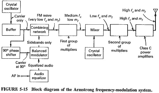
The block diagram of an Armstrong system is shown in Figure 5-15. The system terminates at the output of the combining network; the remaining blocks are included to show how wideband Generation of Frequency Modulation might be obtained. The effect of mixing on an FM signal is to change the center frequency only, whereas the effect of frequency multiplication is to multiply center frequency and deviation equally.
The vector diagrams of Figure 5-16 illustrate the principles of operation of this modulation system. Diagram I shows an amplitude-modulated signal. It will be noted that the resultant of the two sideband frequency vectors is always in phase with the unmodulated carrier vector, so that there is amplitude variation but no phase (or frequency) variation. Since it is phase change that is needed here, some arrangement must be found which ensures that this resultant of the sideband voltages is always out of phase (preferably by 90°) with the carrier vector. If an amplitude-modulated voltage is added to an unmodulated voltage of the same frequency and the two are kept 90° apart in phase, as shown by diagram 2, some form of phase modulation will be achieved. Unfortunately, it will be a very complex and nonlinear form having no practical use; however, it does seem like a step in the right direction. Note that the two frequencies must be identical (suggesting the one source for both) with a phase-shifting network in one of the channels.
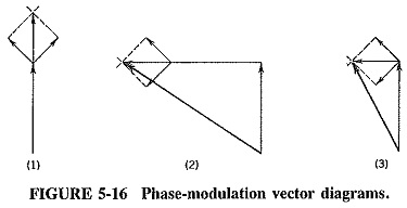
Diagram 3 shows the solution to the problem. The carrier of the amplitude-modulated signal has been removed so that only the two sidebands are added to the unmodulated voltage. This has been accomplished by the balanced modulator, and the addition takes place in the combining network. The resultant of the two sideband voltages will always be in quadrature with the carrier voltage. As the modulation increases, so will the phase deviation, and hence phase modulation has been obtained. The resultant voltage coming from the combining network is phase-modulated, but there is also a little amplitude modulation present. The AM is no problem since it can be removed with an amplitude limiter.
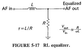
The output of the amplitude limiter, if it is used, is phase modulation. Since Generation of Frequency Modulation is the requirement, the modulating voltage will have to be equalized before it enters the balanced modulator (remember that PM may be changed into FM by prior bass boosting of the modulation). A simple. RL equalizer is shown in Figure 5-17. In Generation of Frequency Modulation broadcasting, ωL= R at 30 Hz. As frequency increases above that, the output of the equalizer will fall at a rate of 6 dB/octave, satisfying the requirements.
Effects of frequency changing on an FM Signal: The previous section has shown that frequency changing of an FM signal is essential in the Armstrong system. For convenience it is very often used with the reactance modulator also. Investigation will show that the modulation index is multiplied by the same factor as the center frequency, whereas frequency translation (changing) does not affect the modulation index.
If a frequency-modulated signal fc ± δ is fed to a frequency doubler, the output signal will contain twice each input frequency. For the extreme frequencies here, this will be 2fc – 2δ and 2fc + 2δ. The frequency deviation has quite clearly doubled to ±2δ, with the result that the modulation index has also doubled. In this fashion, both center frequency and deviation may be increased by the same factor or, if frequency division should be used, reduced by the same factor.
When a frequency-modulated wave is mixed, the resulting output contains difference frequencies (among others). The original signal might again be fc ± δ. When mixed with a frequency f0, it will yield fc – f0 – δ and fc – f0 + δ as the two extreme frequencies in its output. It is seen that the FM signal has been translated to a lower center frequency fc – f0, but the maximum deviation has remained a ± δ. It is possible to reduce (or increase, if desired) the center frequency of an FM signal without affecting the maximum deviation.
Since the modulating frequency has obviously remained constant in the two cases treated, the modulation index will be affected in the same manner as the deviation. It will thus be multiplied together with the center frequency or unaffected by mixing. Also, it is possible to raise the modulation index without affecting the center frequency by multiplying both by 9 and mixing the result with a frequency eight times the original frequency. The difference will be equal to the initial frequency, but the modulation index will have been multiplied ninefold.
Further consideration in the Armstrong system: One of the characteristics of phase modulation is that the angle of phase deviation must be proportional to the modulating voltage. A careful look at diagram 3 of Figure 5-16 shows that this is not so in this case, although this fact was carefully glossed over in the initial description. It is the tangent of the angle of phase deviation that is proportional to the amplitude of the modulating voltage, not the angle itself. The difficulty is not impossible to resolve. It is a trigonometric axiom that for small angles the tangent of an angle is equal to the angle itself, measured in radians. The angle of phase deviation is kept small, and the problem is solved, but at a price. The phase deviation is indeed tiny, corresponding to a maximum frequency deviation of about 60 Hz at a frequency of 1 MHz. An amplitude limiter is no longer really necessary since the amount of amplitude modulation is now insignificant.
To achieve sufficient deviation for broadcast purposes, both mixing and multiplication are necessary, whereas for narrowband FM, multiplication may be sufficient by itself. In the latter case, operating frequencies are in the vicinity of 180 MHz. Therefore, starting with an initial fc = 1 MHz and δ = 60 Hz, it is possible to achieve a deviation of 10.8 kHz at 180 MHz, which is more than adequate for FM mobile work.
The Generation of Frequency Modulation broadcasting station uses a higher maximum deviation with a lower center frequency, so that both mixing and multiplication must be used. For instance, if the starting conditions are as above and 75 kHz deviation is required at 100 MHz, f0 must be multiplied by 100/1 = 100 times, whereas δ must be increased 75,000/60 = 1250 times. The mixer and crystal oscillator in the middle of the multiplier chain are used to reconcile the two multiplying factors. After being raised to about 6 MHz, the frequency-modulated carrier is mixed with the output of a crystal oscillator, whose frequency is such as to produce a difference of 6 MHz/12.5. The center frequency has been reduced, but the deviation is left unaffected. Both can now be multiplied by the same factor to give the desired center frequency and maximum deviation.