Basic Planar Process in IC Fabrication:
The Basic Planar Process in IC Fabrication are as listed below.
- Crystal growth and wafer preparation,
- Epitaxial growth,
- Oxidation,
- Lithography,
- Reactive plasma etching,
- Diffusion,
- Ion implantation,
- Metallization,
- Assembly techniques and packaging
Let us study each process in detail one by one.
Crystal Growth and Wafer Preparation:
In this Basic Planar Process in IC Fabrication following subprocesses, are involved –
- Crystal growing
- Ingot trimming and grinding
- Ingot slicing
- Wafer etching
- Wafer polishing
- Wafer cleaning
Crystal Growth:
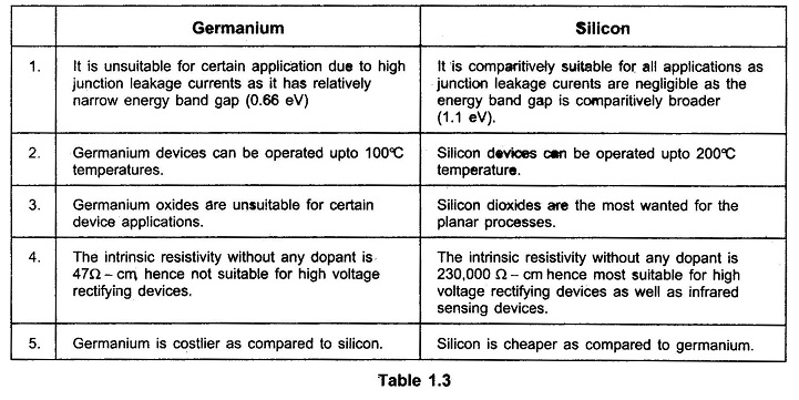
At present 95% of the semiconductor devices use silicon. It occurs naturally in the form of silica and silicates. As we have studied already that the bipolar junction transistor was invented in 1948 with germanium as a semiconductor material. But it was observed that it is advantageous to use silicon than germanium. The table 1.3 gives the comparison between the silicon and germanium material to be used as semiconductor material.
The starting material for the crystal growth is highly purified polycrystalline silicon called as Electronic – Grade Silicon (EGS). To obtain this purest form of silicon, first metallurgical grade silicon (MGS) is produced in a submerged electron arc furnace. Using this step, MGS is solidified with a purity of about 98%. Then the silicon is pulverized mechanically. Then it is added with unhydrous hydrogen chloride to form trichlorosilane (SiHC13). This Basic Planar Process in IC Fabrication is carried out with a catalyst in a fluidized bed at 350°C. After this reaction, the trichlorosilane obtained is liquid at room temperature. Then by using fractional distillation, purification of trichlorosilane is carried out. After this purified trichlorosilane is applied with chemical vapour deposition process. With the help of chemical reaction, hydrogen is reduced from trichlorosilane. It results in the rods of silicon. This multistep process continues for many hours and finally results in polycrystalline structured EGS rods with 0.2 m diameter and several meter length. This process is advantageous because the costing of the process is low and the byproducts of the reactions are less harmful.
The primary method of the crystal growth is Czochralski (CZ) method. In practice all the silicon required for integrated circuits is prepared by using this method only. In general, a phase change from solid, liquid or gas phases to crystalline solid phase is nothing but growing crystal. Czochralski method is used for silicon crystal growth from which ultimately silicon wafers are produced. The apparatus used for the crystal growth is called Czochralski crystal growth apparatus or puller. The puller has four important subsystems namely furnace, crystal pulling mechanism, ambient control and control systems.
The furnace consists a crucible, crucible support, rotation mechanism and heating element housed in a chamber. The crucible is made up of fused silica (SiO2) as this material is chemically unreactive with molten silicon. An EGS block is heated in a fused silica crucible with the appropriate dopant using a heating element. The material in the crucible is heated to a temperature which is greater than the melting point of silicon, i.e. 1417°C. A resistance heating is preferred for large pullers ; while induction heating is used for small melt sizes.
Then a small single crystal rod of silicon is immersed into the molten material. This rod is called seed crystal. This seed crystal is located at the crystal pulling assembly. In this assembly, using rotating mechanism seed shaft and seed chuck are rotated. Lowering the seed crystal in molten silicon allows the crystal ingot to form on the seed by solidification. The main function of crystal pulling assembly, is to control the pull rate of seed crystal and crystal rotation both, with minimum vibrations and precision. During the crystal growth, the crystal is rotated slowly, by stirring the molten and averaging out temperature gradients leading to inhomogeneous solidification. To get the ingots of circular cross-section, the crucible and the seed crystal are rotated in opposite direction. When the seed crystal is pulled out of the molten material, due to solidification, silicon ingot gets formed exactly same as seed crystal.
In general, the diameter is controlled by the pull rate. The standard diameter of the ingot is about 150 mm and the length is about 2m. The ingot with such dimensions weighs about 60 kg.
The silicon growth is generally conducted in a vacuum or in an inert gas like helium or argon.
To control the process parameters such as temperature, crystal diameter, pull rate and rotation speed etc, control system is used which works under either open loop control or closed loop control.
Ingot Trimming and Grinding:
First of all, the seed which initiated the crystal growth is separated from the circular ingot. The top and bottom ends are also cut off. As silicon is hard and brittle material, industrial grade diamond is used for shaping and cutting it. After completion of the crystal growth, it is generally tested for resistivity and perfection evaluation. So the portions of the ingot failed in the above tests are also cut. Note that these cuttings can be recycled for new crystal growth after cleaning.
After trimming of the ingot, the surface grinding of the ingot is carried out. Actually the ingots are slightly oversized. Hence with the help of lathelike diamond tool, the ingot is ground to a precise diameter.
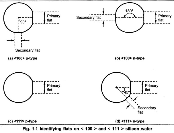
After grinding the ingot to a precise diameter, generally two flats are ground along the length of the ingot. The larger flat is called major or primary flat and it is positioned relative to the crystal direction. The x-ray technique is used to locate the primary flat. The primary flat is very important as
- it serves for mechanical alignment of the wafer in automatic processing, and
- it serves for orienting ICs on the wafer relative to the crystal.
The smaller flat is called secondary flat which is used to identify the orientation (< 100 > or < 111 >) and conductivity (p or n) of the wafer.
Ingot Slicing:
Once the flats have been ground, the ingot is sliced into wafers. This process is very important because it is necessary to maintain the flat plane and desired surface orientations.
The slicing also determines the orientation of the surface. In general, there are two orientations < 100 > and < 111 >. Out of these orientations, the wafers with < 100 > orientations are cut ‘on orientation’ ; while wafers with < 111 > orientations are cut ‘off orientations’. The position of the flats can be identified according to the standards laid by the Semiconductor Equipment and Materials Institute (SEMI) as shown in the Fig. 1.1.
The ingot is sliced using a circular cutting blade kept in tension on the outer edge while having the cutting edge on the inner diameter.
The thickness of the wafer is determined by the slicing. It is another important wafer parameter because thicker wafers can easily withstand the stresses of subsequent thermal processes. The higher quality of slicing is achieved by using capacitive sensing device near the blade which helps the blade to be positioned correctly to achieve exactly flat plane cut.
Wafer Etching:
If the sliced wafers are to be used for VLSI application, then before etching process two sided mechanical lapping process is carried out. Using this process, wafers with uniform flatness are achieved which are mostly required for photolithography.
Due to the machining operations during trimming, grinding and slicing, the surface and edges of the wafers get contaminated and even damaged. The depth of damage depends on the mechanical operations carried previously. It is observed that the damaged and contaminated regions are not more than 10 μm deep. Even by using chemical etching process, all the damaged and contaminated edges can be removed. Practically mixture of hydrofluoric, acetic and nitric acids is used in chemical etching. This is called acidic etching. The other alternative is to use alkaline etching using potassium hydroxide or sodium hydroxide. By the etching process, typically 10 μm to 30 μm of wafer is removed from both the sides.
Wafer Polishing:
After etching, the wafer is polished to eliminate the microcracks and debris. The main intension of polishing a wafer is to provide a smooth and perfect flat surface such that the device features can be engraved. The polishing is done with the help of a polishing machine. Note that the polishing process removes further 10 μm to 30 μm of the wafer surface typically.
The three steps of lapping, etching and polishing reduce the wafer thickness by 40 to 150 μm. Thus by considering the typical figures, to have the wafer of 200 μm thickness, the thickness of the substrate required is 560 μm, In practice, the processed 6 inch wafers are typically 250 μm to 500 μm thick.
Wafer Cleaning:
The silicon wafers are cleaned using chemicals. Generally organic films, heavy metals are deposited on the surface of the wafers. Hence by using HC1 – H2O2. aqueous solution, metallic impurities can be removed. First the wafer is cleaned by using HC1 – H2O2. Then wafer is rinsed in water to deionize. Again the wafer is dipped in hydrofluoric acid. Then again the wafer is rinsed in water.
After cleaning process, the wafer is ready for the formation of the dies.
Epitaxy:
The epitaxy means ‘arranged upon’. In epitaxy a monocrystalline film is formed on the top of a monocrystalline surface. Thus epitaxy is crystalline growth process in which the foundation layer i.e. substrate works as seed crystal. The epitaxial layer formed on the substrate may be either n-doped, p-doped or intrinsic. The polarity and the concentration of the dopant to be used is not determined by the foundation layer. In general for p-type doping bi-borane (B2H6) and for n-type doping phosphine (PH3) are used with the steam of silicon tetrachloride hydrogen gas.
There are two types of epitaxy as given below.
Homoepitaxy : When the epitaxial layer and the substrate on which the epitaxial layer is to be formed, are of same materials, then the process is called Homoepitaxy. The silicon process in which silicon is grown or formed over silicon substrate is an example of homoepitaxy.
Heteroepitaxy : When the epitaxial layer and the substrate on which the epitaxial layer is to be formed are not of identical material, then the process is called heteroepitaxy. But for crystalline growth with heteroepitaxy, the materials must have identical crystal structure.
While studying epitaxy one must note that this process is not restricted to a single layer formation on the substrate. But multiple epitaxial layers are also possible which are widely found in various applications such as microwave p-i-n diodes.
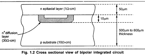
In general bipolar integrated circuits use epitaxial layer process in which high resistivity epitaxial layer is formed over a low resistivity substrate. To provide isolation between the epitaxial growth and the substrate, the doping used in both layers is of opposite type. Due to this a heavily doped buried layer is formed. The buried layer is also called diffusion layer as shown in the Fig. 1.2.
The advantages of epitaxy are
- Because of one or more buried layers, the designer can control the doping in the structure.
- The properties of the epitaxial layer and the bulk material are different.
- Using epitaxial structures the performances of RAMs (Random access memories) and CMOS ICs can be improved.
The two main epitaxial processes are
- Chemical vapour deposition (CVD) and
- Molecular beam epitaxy (MBE)