Integrated Circuit Operational Amplifier:
Circuit Symbol and Packages – Figure 14-1(a) shows the triangular circuit symbol for an Integrated Circuit Operational Amplifier (op-amp). As illustrated, there are two input terminals, one output terminal, and two supply terminals. The inputs are identified as the inverting input (- sign) and the noninverting input (+ sign). A positive-going voltage at the inverting input produces a negative-going (inverted) voltage at the output terminal. Conversely, a positive-going voltage at the noninverting input generates an output which is also positive-going (noninverted). Plus-minus supplies are normally used with op-amps, so the supply terminals are identified as +VCC and -VEE.
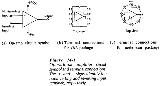
Two typical op-amp packages are illustrated in Figs. 14-1 (b) and (c). For both the dual-in-line (DIL) plastic package and the metal can package, terminals 2 and 3 are the inverting and noninverting inputs respectively, terminal 6 is the output, and terminals 7 and 4 are the + and – supply terminals.
Basic Op-Amp Circuit:
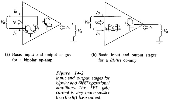
The input and output stages for bipolar and BIFET operational amplifiers shown in Figs. 14-2(a) and (b). The differential-amplifier input stage has two (inverting and noninverting) high-impedance input terminals, and the emitter follower output stage has a low impedance. An intermediate stage (between the input and output stages) is largely responsible for the op-amp high voltage gain. Figure 14-2(a) shows a BJT input stage, while Fig. 14-2(b) has a FET input stage. Appropriately, op-amps that exclusively use BJTs are termed bipolar op-amps, and those that use a FET input stage with BJT additional stages are referred to as BIFET op-amps.
Important Parameters:
Some of the most important parameters for the 741 Integrated Circuit Operational Amplifier (one of the most commonly used) are listed in the data sheet portion shown in Fig. 14-3.
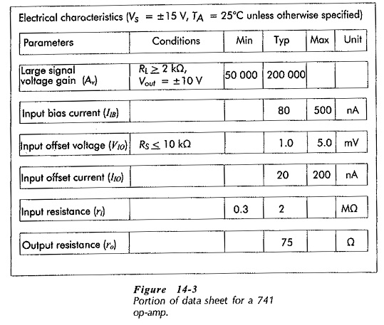
The large signal voltage gain (Av), also identified as the open-loop gain Av(OL)), for the 741 is listed as as 50 000 minimum and 200 000 typical. This means, for example, that a signal applied as a voltage difference between the two input terminals is amplified at least by a factor 50 000. The typical amplification is 200 000, and the maximum amplification can be considerably greater. This is similar to the situation with the hfe of a BJT, where the manufacturer specifies minimum, typical, and maximum values.
The input bias current (IIB) is the base current for the op-amp input stage transistors. In Fig. 14-3 IIB is listed as 80 nA typical, and 500 nA maximum.
Ideally, the input stage transistors should be perfectly matched, so that zero voltage difference between the two input (base) terminals should produce a zero output voltage. In practice, there is always some difference between the base-emitter voltages of the transistors, and this results in an input offset voltage (VIO), that might be as large as 5 mV for a 741 op-amp. Similarly, because of mismatch of input transistors, there is also an input offset current (IIO). For the 741 IIO is a maximum of 200 nA.
The input resistance (ri) and the output resistance (ro) are the resistances at the op-amp terminals when no feedback is involved. Virtually all op-amp applications use negative feedback, so these (resistance) quantities are modified in practical circuits.
The dc supply voltage for electronic circuits can vary when the supply current changes, and in some cases there is an ac ripple voltage superimposed on the dc. The supply voltage changes can be passed to the output of an amplifier. Ideally, the supply voltage variations should have no effect on the circuit output. How good the amplifier is at attenuating supply voltage variations is defined by the power supply voltage rejection ratio (PSRR). This is usually specified in decibel form.
Common mode inputs are voltage changes that are applied simultaneously to both input terminal of an Integrated Circuit Operational Amplifier. Common mode input voltages can be passed to the output. The common mode rejection ratio (CMRR) (expressed in dB) defines how good the amplifier is at attenuating common mode input voltages.