Complementary MOSFET Common Source Power Amplifier:
Advantages of MOSFETs:
Complementary MOSFET Common Source Power Amplifier have several advantages over power BJTs for large signal amplifier applications. One of the most important differences is that MOSFET transfer characteristics (ID/VGS) are more linear than IC/VBE characteristics for BJTs. This helps to minimize distortion in the output waveform. Thermal runaway does not occur with power MOSFETs, so the emitter resistors in the BJT output stage are not needed in a MOSFET amplifier. Thus, the wasted power dissipation in the emitter resistors is eliminated.
Power MOSFETs can be operated in parallel to reduce the total channel resistance and increase the output current level. Unlike BJTs operated in parallel, there is no need for resistors to equalize current distribution between parallel-connected MOSFETs. For Class-AB operation, the MOSFET gate-source should be biased to the threshold voltage (VTH) for the device, to ensure that it is conducting at a low level when no signal Is present.
Power Amplifier with MOSFET Output Stage:
The four output transistors in the amplifier circuit could be replaced with two power MOSFETs operating as source followers. However, the FET gate-source voltage must be included when calculating the supply voltage, so that a larger supply voltage would be required than with a BJT amplifier. In the power amplifier in Fig. 18-36 the complementary MOSFETs output devices operate as Complementary MOSFET Common Source Power Amplifier. As will be seen, this permits the peak output voltage to approach the supply voltage level.
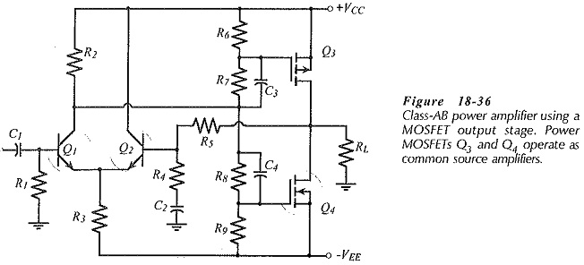
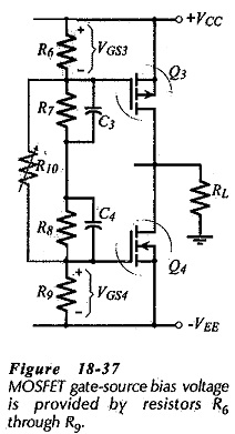
As in the case of the BJT circuit, the differential amplifier input stage in Fig. 18-36 allows the use of do negative feedback (via R5) to stabilize the do output voltage level, and ac negative feedback (via R4 and R5) to set the closed-loop voltage gain. Output transistors Q3 and Q4 are complementary MOSFETs and both are operated as Complementary MOSFET Common Source Power Amplifier. Resistors R6 through R9 provide bias voltage to set the gate-source voltage of Q3 and Q4 to the threshold level (VTH) for the MOSFETs, (see Fig. 18-37). Resistors R10 can be included, as shown, to facilitate bias voltage adjustment. Capacitors C3 and C4 short-circuit R7 and R8 at signal frequencies, so that all of the ac voltage from the first stage is applied to the MOSFET gate terminals.
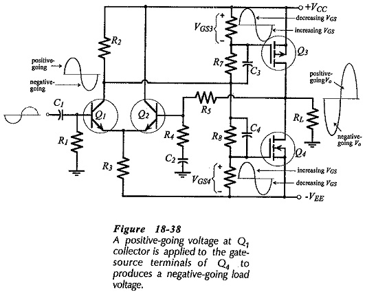
A positive-going voltage at Q1 collector increases VGS4 and decreases VGS3. Thus, Q4 drain current is increased and Q3 is turned off, (see Fig. 18-38). ID4 flows through RL producing a negative-going load voltage. When the voltage at Q1C is negative-going, VGS4 is decreased and VGS3 is increased. This causes ID3 to increased and Q4 to be turned off. Load current now flows via Q3 to produce a positive-going load voltage.
MOSFET Power Amplifier Design:
In a Class-AB MOSFET power amplifier, the FET gate-source voltages should be biased to the minimum specified threshold voltage for the devices. The peak output voltage and current are calculated in the usual way, and the minimum supply voltage is,
![]()
where RD(on) is the FET channel resistance.
The required gate-source voltage swing (ΔVGS) is determined from Ip/gFS. The input stage must provide for ±ΔVGS at Q1 collector (Fig. 18-38). Power dissipation in Q3 and Q4 is determined in the same way as for a BJT stage. The selected MOSFETs must survive the total supply voltage and pass a drain current approximately equal to 1.1 Ip. Capacitor values are determined in the usual way.