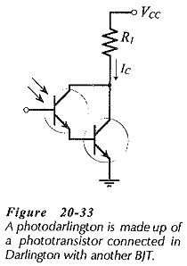
Photodarlington Working:
The Photodarlington Working shown in (Fig. 20-33) consists of a phototransistor connected in Darlington arrangement with another transistor. This device is capable of producing much higher output currents than a phototransistor, and so it has a greater sensitivity to illumination levels than either a phototransistor or a photodiode. With the additional transistor involved, the Photodarlington Working has a considerably longer switching time than a phototransistor.
PhotoFET:
A photoFET is a JFET designed to have its gate-channel junction illuminated. The illumination controls the level of the device drain current. Consider the n-channel JFET and the photoFET in Fig. 20-34. The gate-source leakage current (IGSS) is the reverse saturation current at a pn-junction.
The voltage drop across RG produced by IGSS is normally too small to affect the JFET circuit. In the photoFET, the junction reverse current (λIG) is susceptible to light. Illumination on the junction generates additional minority charge carriers, thus increasing λIG. This current flows through the bias resistance (RG) and produces a voltage drop (VRG), as illustrated.
If the gate bias voltage (-VG) is just sufficient to bias the device off when dark, then when the junction is illuminated, VRG can raise the level of the gate voltage to bias the photoFET on.
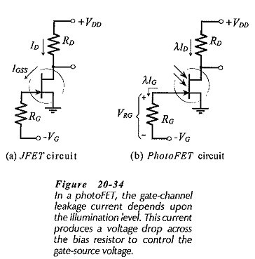
The external bias voltage (-VG) might be selected at a level that biases the device on, so that light level variations cause ID to increase and decrease. In a photoFET, λIG is termed the gate current, and the normal IGSS at the junction is the dark gate-leakage current. The light-controlled drain current is designated λID.