Gunn Effect:
In 1963, Gunn discovered the transferred electron effect which now bears his name. This Gunn Effect is instrumental in the generation of microwave oscillations in bulk semiconductor materials. The effect was found by Gunn to be exhibited by gallium arsenide and indium phosphide, but cadmium telluride and indium arsenide have also subsequently been found to possess it. Gunn Effect discovery was a breakthrough of great importance. It marked the first instance of useful semiconductor device operation depending on the bulk properties of a material.
Introduction:
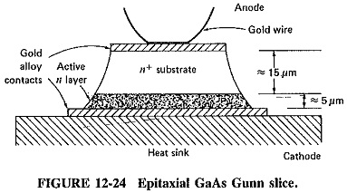
If a relatively small dc voltage is placed across a thin slice of gallium arsenide, such as the one shown in Figure 12-24, then negative resistance will manifest itself under certain conditions. These consist merely of ensuring that the voltage gradient across the slice is in excess of about 3300 V/cm. Oscillations will then occur if the slice is connected to a suitably tuned circuit. It is seen that the voltage gradient across the slice of GaAs is very high. The electron velocity is also high, so that oscillations will occur at microwave frequencies.
It must be reiterated that the Gunn effect is a bulk property of semiconductors and does not depend, as do other semiconductor effects, on either junction or contact properties. As established painstakingly by Gunn Effect, the effect is independent of total voltage or current and is not affected by magnetic fields or different types of contacts. It occurs in n-type materials only, so that it must be associated with electrons rather than holes. Having determined that the voltage required was proportional to the sample length, the inventor concluded that the electric field, in volts per centimeter, was the factor determining the presence or absence of oscillations. He also found that a threshold value of 3.3 kV/cm must be exceeded if oscillations are to take place. He found that the frequency of the oscillations produced corresponded closely to the time that electrons would take to traverse such a slice of n-type material as a result of the voltage applied. This suggests that a bunch of electrons, here called a domain, is formed somehow, occurs once per cycle and arrives at the positive end of the slice to excite oscillations in the associated tuned circuit.
Negative Resistance:
Although the device itself is very simple, its operation (as might be suspected) is not quite so simple. Gallium arsenide is one of a fairly small number of semiconductor materials which, in an n-doped sample, have an empty energy band higher in energy than the highest filled (or partly filled) band. The size of the forbidden gap between these two is relatively small. This does not apply to some other semiconductor materials, such as silicon and germanium. The situation for gallium arsenide is illustrated in Figure 12-25, in which the highest levels shown also have the highest energies.
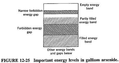
When a voltage is applied across a slice of GaAs which is doped so as to have excess electrons (i.e., n-type), these electrons flow as a current toward the positive end of the slice, The greater the potential across the slice, the higher the velocity with which the electrons move toward the positive end, and therefore the greater the current. The device is behaving as a normal positive resistance. In other diodes, the component of velocity toward the positive end, imparted to the electrons by the applied voltage, is quite small compared to the random thermal velocity that these electrons possess. In this case, so much energy is imparted to the electrons by the extremely high voltage gradient that instead of traveling faster and therefore constituting a larger current, their flow actually slows down. This is because such electrons have acquired enough energy to be transferred to the higher energy band, which is normally empty, as shown in Figure 12-25. This gives rise to the name transferred-electron effect, which is often given to this phenomenon. Electrons have been transferred from the conduction band to a higher energy band in which they are much less mobile, and the current has been reduced as a result of a voltage rise. Note that, in a sense, gallium arsenide is a member of a group of unusual semiconductor substances. In a lot of others, the energy, required for this transfer of electrons would be so high, because of a higher forbidden energy gap, that the complete crystal structure might be distorted or even destroyed by the high potential gradient before any transfer of electrons could take place.
It is seen that as the applied voltage rises past the threshold negative-resistance value, current falls, and the classical case of negative resistance is exhibited. Eventually the voltage across the slice becomes sufficient to remove electrons from the higher-energy, lower-mobility band, so that current will increase with voltage once again. The voltage-current characteristic of such a slice of gallium arsenide is seen to be very similar to that of a tunnel diode, but for vastly different reasons.
Gunn Domains:
It was stated in the preceding section that the oscillations observed in the initial GaAs slice were compatible with the formation and transit time of electron bunches. It follows, therefore, that the negative resistance just described is not the only effect taking place. The other phenomenon is the formation of domains, the reasons for which may now be considered.
It is reasonable to expect that the density of the doping material is not completely uniform throughout our sample of gallium arsenide. Hence it is entirely possible that there will be a region, perhaps somewhere near the negative end, where the impurity concentration is less than average. In such an area there are fewer free electrons than in other areas, and therefore this region is less conductive than the others. As a result of this, there will be a greater than average potential across it. Thus, as the total applied voltage is increased, this region will be the first to have a voltage across it large enough to induce transfer of electrons to the higher energy band. In fact, such a region will have become a negative-resistance domain.
A domain like this is obviously unstable. Electrons are being taken out of circulation at a fast rate within it, the ones behind bunch up and the ones in front travel forward rapidly. In fact, the whole domain moves across the slice toward the positive end with the same average velocity as the electrons before and after it, about 107 cm/s in practice. Note that such a domain is self-perpetuating. As soon as some electrons in a region have been transferred to the less conductive energy band, fewer free electrons are left behind. Thus this particular region becomes less conductive, and therefore the potential gradient across it increases. The domain is quite capable of traveling and may be thought of as a low-conductivity, high-electron-transfer region, corresponding to a negative pulse of voltage. When it arrives at the positive end of the slice, a pulse is received by the associated tank circuit and shocks it into oscillations. It is actually this arrival of pulses at the anode, rather than the negative resistance proper, which is responsible for oscillations in Gunn Effect diodes. (The term diode is a misnomer for Gunn Effect devices since there is no junction, nor is rectification involved. The device is called a diode because it has two terminals, and the name is also convenient because it allows the use of anode for the “positive end of the slice. ”)
With the usual applied voltages, once a domain forms, insufficient potential is left across the rest of the slice to permit another domain to form. This assumes that the sample is fairly short; otherwise the situation can become very complex, with the possibility that other domains may form. The domain described is sometimes called a dipole domain. An accumulation domain may also occur (particularly in a longer sample), where a more highly doped region is involved, and a current accumulation travels toward the anode. When the domain in a short sample arrives at the anode, there is once again sufficient potential to permit the formation of another domain somewhere near the cathode. It is seen that only one domain, or pulse, is formed per cycle of RF oscillations, and so energy is received by the tank circuit in correct phase to permit the oscillations to continue.
Miscellaneous Considerations:
The following brief notes and observations are now made:
-
The Gunn diode/oscillator has received various names. Although Gunn (diode or oscillator) will always be used here, students should be aware of names such as transferred-electron devices (or TED) and transferred-electron oscillator (or TEO), which are also frequently used.
- The Gunn effect is eminently viable, and Gunn diodes are very widely used.
- Although only gallium arsenide diodes have been considered, indium phosphide (InP) Gunn diodes are becoming widely used, especially at the highest frequen InP has properties quite similar to those of GaAs, while also offering the advantages of a higher peak-to-valley ratio in its negative resistance characteristic and lower noise.
-
Students must surely be wondering by now why such “oddball” operating principles are used by the majority of solid-state microwave devices and they have not even encountered the IMPATT diode as yet! The only explanation the author can put forward is that all the simple devices got themselves invented a long time ago, and they didn’t work at microwave frequencies!