FET Biasing Articles:
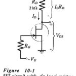
DC Load Line for FET: The DC Load Line for FET circuit is drawn on the device output characteristics (or drain characteristics) in exactly the same way as for a BJT circuit. Refer to the n-channel FET circuit in Fig. 10-1. … (Read More)
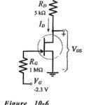
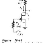
Gate Bias Circuit: Circuit Operation – Consider the Gate Bias Circuit shown in Fig. 10-6. The FET gate terminal is connected via resistor RG to a bias voltage VG. If the gate is directly connected to the bias source (instead of … (Read More)
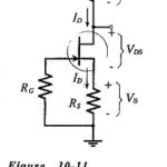
Self Bias Circuit Diagram: Circuit Operation – In a self bias JFET circuit, gate-source bias is provided by the voltage drop across a resistor in series with the device source terminal. Consider the n-channel JFET Self Bias Circuit Diagram illustrated in … (Read More)
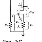
Voltage Divider Bias Circuit: For the self-bias circuit, it was seen that increasing the resistance of RS brings ID(max) and ID(min) closer together, but that increased RS values result in lower ID levels. As will be demonstrated, Voltage Divider Bias Circuit allows RS … (Read More)
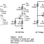
Basic JFET Biasing Circuits Comparison: The Basic JFET Biasing Circuits Comparison (gate bias, self-bias, and voltage divider bias) are similar in performance to the three basic BLIP bias circuits, (base bias, collector-to-base bias, and voltage divider bias). Comparing the performance of … (Read More)
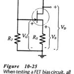
JFET Bias Circuit Troubleshooting: Voltage Measurement – JFET Bias Circuit Troubleshooting are similar to those for BJT bias circuits. The major difference is that there is only one junction in the FET (the gate-channel junction) that might become short-circuited or open-circuited. … (Read More)
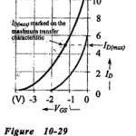
JFET Bias Circuit Design: Design Approach – Design of JFET Bias Circuit Design is just as simple as design of BJT bias circuits. One major difference is that FET circuit design normally uses a graphical approach involving the drawing of a … (Read More)
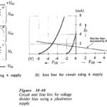
JFET Biasing Circuits: Use of Plus/Minus Supplies – When plus/minus supply voltages are to be used with a JFET Biasing Circuits, the gate terminal is usually grounded via RG, as illustrated in Fig. 10-40(a). In this case, the circuit is essentially … (Read More)
Universal Transfer Characteristics for FET: A Universal Transfer Characteristics for FET is simply a transfer characteristic plotted with IDSS = 1 and VP = 1. Then, instead of the scales being calibrated in milliamps and volts, they are marked as the ratios ID/IDSS and VGS/VP. To … (Read More)
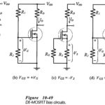
MOSFET Biasing Circuits: DE-MOSFET Bias Circuits – DE-MOSFET bias circuits are similar to JFET bias circuits. Any of the FET bias circuits already discussed can be used to produce a negative VGS level for an n-channel MOSFET Biasing Circuits, or a … (Read More)
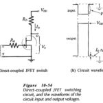
Biasing FET Switching Circuits: JFET Switching – A Biasing FET Switching Circuits is normally in an off state with zero drain current, or in an on state with a very small drain-source voltage. When the FET is off, there is a … (Read More)