DA Converter Working Principle:
The resistive divider or ladder can be used as the basis for a DA Converter Working Principle. It is in the resistive network that the actual translation from a digital to an analog signal voltage takes place. However, there is a need for additional circuitry to complete the design of a D/A converter.
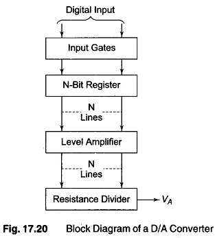
An integral part of a D/A converter is a register which can be used to store digital information. The simplest register is formed using an RS flip-flop, with one F/F per bit. There must also be a level amplifier between the register and the resistive network, to ensure that the digital signals presented to the network are all of the same levels and are constant. Finally there must be some form of gating on the input of the register, such that the F/F’s can be set with the proper information from the digital system. A basic block diagram of a D/A converter is shown in Fig. 17.20, and a complete block diagram of a 4-bit DA Converter Working Principle is shown in Fig. 17.21.
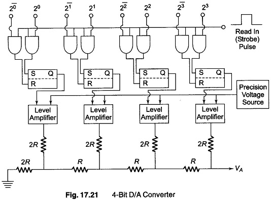
The resistive network used is of the ladder type. The level amplifiers have two input each. One input is the +10 V from the precision voltage source, and the other is from an F/F. The amplifier works in such a way that when the input from an F/F is high, the output of the amplifier is at +10, and when the input from the F/F is low, the output is 0 V.
Four F/Fs used form the register necessary for storing the digital information. The F/F on the right represents the MSB and the F/F on the left LSB. Each F/F is a simple RS type F/F and requires a + ve level at R or S inputs to
reset or set it.
When the read line goes high, one of the two gates connected to the F/F is true (enabled) and the F/F sets or resets accordingly. Hence data are entered into the register each time the read in (strobe) pulse occurs.
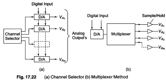
Quite often it is necessary to decode more than one signal, e.g. X — Y coordinates for a plotter. There are two methods of decoding these signals.
- The first method, is to simply use a D/A converter for each signal, as shown in Fig. 17.22 (a). This has the advantage that each signal to be decoded is held in its register and the analog output voltage is then held fixed. The digital input lines are connected in parallel to each converter. The proper converter is then selected for decoding by the select lines.
- The second method involves using only one D/A converter and switching its output. This is called multiplexing, and is shown in Fig. 17.22 (b). The disadvantage here is that the analog output signal must be held between sampling periods and the outputs must therefore be equipped with sample hold circuits.
A sample hold amplifier can be approximated by a capacitor and high gain opamp, as shown in Fig. 17.23.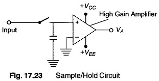
When the switch is closed, the capacitor charges to the D/A converter output voltage. When the switch is opened, the capacitor holds the voltage level until the next sampling time. The opamp provides a large input impedance, so that the capacitor is not discharged appreciably and at the same time offers gain to drive external circuits.
When the D/A converter is used in conjunction with a multiplexer, the maximum rate at which the converter can operate must be considered. Each time data is shifted into the register, transients appear at the output of the converter. This is due to the different rise and fall of each F/.F. Hence, a settling time must be allowed between the time data is shifted into the register, and the time the analog voltage is read out. The settling time is the main factor in determining the maximum rate at which the output can be multiplexed. The worst case is when all bits change (i.e. from 1000 to 0111). The sampling rate is a function of the capacitors, as well as the frequency of the analog signal which is expected at the output of the converter.