Op Amp Comparator Circuit:
Op Amp Comparator Circuit – In the opamp applications discussed so far, the amplifiers use negative feedback. Under normal conditions, when negative feedback is used in such a circuit, the amplifier output voltage takes on values between the positive and negative saturation limits. The amplifier has a high gain and negative feedback forces the voltage between the differential input to be small at all times.
When opamp is used without feedback (open loop operation), the amplifier output is usually in one of its saturated states. The application of a small difference input signal of appropriate polarity causes the output to switch to its other saturation states.
Therefore, a Comparator is a circuit with two inputs and a single output. The two inputs can be compared with each other, i.e., one of them can be considered a reference terminal.
When the non-inverting input is higher or greater than the inverting input voltage, the output of the comparator is high and when the non-inverting voltage is less than the latter output of the Comparator is low.
If the inverting terminal is grounded, even the slightest input voltage at the non-inverting terminal is enough to saturate the opamp. Therefore, the output is at positive saturation as soon as the voltage at the non-inverting terminal increases slightly above zero.
Similarly, the opamp goes to negative saturation, as soon as the voltage at the non-inverting terminal goes slightly below ground level.
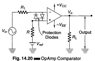
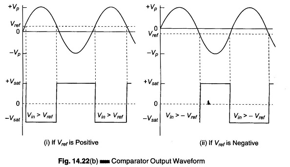
The Op Amp Comparator Circuit shown in Fig. 14.20, consists of a fixed reference voltage (Vref) applied to the inverting input terminal and a sinusoidal signal Vin applied to the non-inverting terminal. As discussed earlier, when Vin is greater than Vref, the output voltage goes to positive saturation, i.e. Vout = +Vsat = +Vcc and when Vin is less than Vref, the output goes to negative saturation, i.e. Vout = – Vsat = – VEE.
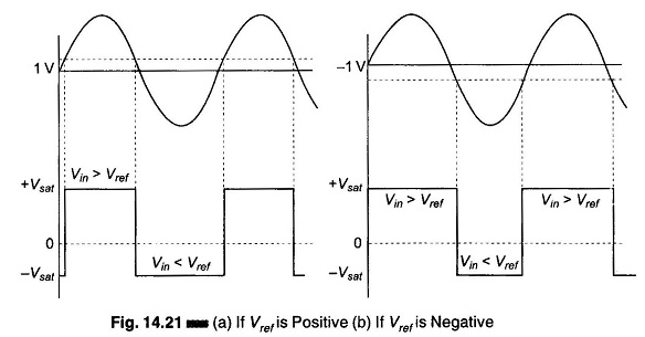
Hence the output changes from one saturation level to another whenever Vin ≡ Vref, as shown in Fig. 14.21.
Since the sinusoidal input is applying to the non-inverting terminal, this circuit is called the non-inverting comparator.
Similarly, an inverting comparator can also be obtained by applying the sinusoidal input to the inverting terminal.
Diodes D1 and D2, shown in Fig. 14.20 are used to protect the opamp from damage due to excessive input voltage (Vin). The difference input voltage (Vid) of the opamp is clamped to either + 0.7 V or – 0.7 V because of the diodes D1 and D2. Hence the diodes are called clamping diodes.
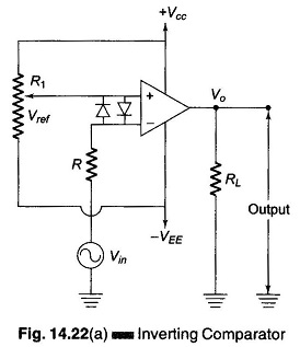
Figure 14.22 (a) shows the circuit for an inverting comparator, the input-output waveforms are shown in Fig. 14.22. (b). In this circuit, Vref is obtained by the use of a potentiometer which forms a potential divider arrangement. Op Amp Comparator Circuits are used as discriminators, voltage level detectors, oscillators, digital interfacing, Schmitt trigger, etc.